To understand how to reduce power in memory, we must first understand the current memory technologies and the interactions between memory and the rest of the system.
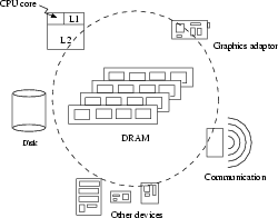
Since 1980, processor speeds have been improving at an annual rate of 80%, while Dynamic Random Access Memory (DRAM) only improved at an annual rate of 7% [39]. Even with a cache hierarchy sitting between the memory and the processor, hiding some of the latencies, the performance gap between the memory and the processor is continuously widening. Memory also interacts with various other system components, such as hard disks, video adapters, and communication devices that use DMA to transfer data as shown in Figure 1. Therefore, memory performance has a significant impact on the overall system performance. Since power reduction is only possible when the memory is operating at lower performance levels, it is critical to implement power-management techniques so that the power reduction in memory justifies any performance degradation, or even power increase, in other system components.
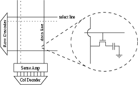
DRAM memory consists of large arrays of cells, each of which uses a transistor-capacitor pair to store a single bit as shown in Figure 2. To counter current leakage, each capacitor must be periodically refreshed to retain its bit information, making memory a continuous energy consumer. Because DRAM fabrication uses advanced process technologies that allow high-capacitance and low-leakage circuits, this refresh occurs relatively infrequently, and is not the largest consumer of DRAM power. Due to the large arrays with very long, highly-loaded internal bus lines, and high degree of parallel operations, significant energy is consumed by row decoders, column decoders, sense amplifiers, and external bus drivers. To reduce power, when a device is not actively being accessed, we can put it into lower power levels by disabling some or all of these subcomponents. However, when it is accessed again, a performance penalty is incurred for transitioning from a low-power mode to an active mode by re-enabling these components. This is due to the time needed to power up bus and sense amplifiers, and synchronize with the external clock, and so this time penality is called a resynchronization cost. This non-negligible resynchronization cost is the source of performance degradation when power management is not carefully implemented.
 |
The above holds true for all Synchronous DRAM (SDRAM) architectures including the single-data-rate (SDR), the double-data-rate (DDR), and the recently-introduced Rambus (RDRAM) architectures. However, for our energy-conservation purposes, RDRAM differs from the rest by allowing a finer-grained unit of control in power management. In this paper, we consider all three memory types, and show that a finer-grained control can save a significant amount of additional energy over the coarser-grained traditional memory architectures. We now look more closely at these memory architectures with respect to power dissipation.