16th USENIX Security Symposium
Pp. 87–102 of the Proceedings
Keep your enemies close:
Distance bounding against smartcard relay attacks
Modern smartcards, capable of sophisticated cryptography, provide a high assurance of tamper resistance and are thus commonly used in payment applications.
Although extracting secrets out of smartcards requires resources beyond the means of many would-be thieves, the manner in which they are used can be exploited for fraud.
Cardholders authorize financial transactions by presenting the card and disclosing a PIN to a terminal without any assurance as to the amount being charged or who is to be paid, and have no means of discerning whether the terminal is authentic or not.
Even the most advanced smartcards cannot protect customers from being defrauded by the simple relaying of data from one location to another.
We describe the development of such an attack, and show results from live experiments on the UK's EMV implementation, Chip & PIN.
We discuss previously proposed defences, and show that these cannot provide the required security assurances.
A new defence based on a distance bounding protocol is described and implemented, which requires only modest alterations to current hardware and software.
As far as we are aware, this is the first complete design and implementation of a secure distance bounding protocol.
Future smartcard generations could use this design to provide cost-effective resistance to relay attacks, which are a genuine threat to deployed applications.
We also discuss the security-economics impact to customers of enhanced authentication mechanisms.
1 Introduction
Authentication provides identity assurance for, and of, communicating parties.
Relay, or wormhole attacks allow an adversary to impersonate a participant during an authentication protocol by effectively extending the intended transmission range for which the system was designed.
Relay attacks have been described since at least 1976 [13, p75] and are simple to execute as the adversary does not need to know the details of the protocol or break the underlying cryptography.
A good example is a relay attack on proximity door-access cards demonstrated by Hancke [16].
To gain access to a locked door, the adversary simply relays the challenges from the door to an authorized card, possibly some distance away, and sends the responses back.
The only restriction on the attacker is that the signals arrive at the door and remote card within the allotted time, which Hancke showed to be sufficiently liberal.
Another example is wormhole attacks on wireless networks by Hu et al. [18].
Despite the existence of such attacks, systems susceptible to them are regularly being deployed.
One significant reason is that designers consider relay attacks to be too difficult and costly for attackers to deploy.
sec:relay aims to show that relay attacks are indeed practical, using as an example the UK's EMV payment system, Chip & PIN.
These flaws are demonstrated by an implementation of the relay attack that has been tested on live systems.
Once designers appreciate the risk, the next step in building a secure system is to develop defences.
sec:defences describes potential countermeasures to the relay attack and compares their cost and effectiveness.
While some, which depend on procedural changes, could be deployed quickly and act as an interim measure, none of the conventional technologies meet our requirements of adequate security at low cost.
We thus propose an extension to the smartcard standard, based on a distance bounding protocol, which provides adequate resistance to the relay attack and requires minimal changes to smartcards.
sec:distance describes this countermeasure and its relationship with prior work, describes a circuit design, and evaluates its performance and security properties. We have implemented the protocol on an FPGA and shown it to be an effective defence against very capable adversaries.
In addition, the experience of both users and merchants is unchanged, a significant advantage over the other proposals we discuss. The impact of this protocol on the fraud liability landscape is discussed in sec:discussion.
Our contributions include the description of the practicalities of relay attacks and our confirmation that deployed systems are vulnerable to them.
By designing and testing a prototype system for demonstrating this vulnerability, we show that the attack is feasible and an economically viable threat.
Also, we detail the design of a distance bounding protocol for smartcards, discuss implementation issues and present results from both normal operation and under simulated attacks.
While papers have previously discussed distance bounding protocols, to the best of our knowledge, this is the first time it has been implemented in practice.
2 Background
Contact smartcards, also known as integrated circuit cards (ICC), as discussed in this paper, are defined by ISO 7816 [19] (for brevity, our description of the specification will be only to the detail sufficient to illustrate our implementation).
The smartcard consists of a sheet of plastic with an integrated circuit, normally a specialized microcontroller, mounted on the reverse of a group of eight contact pads.
Current smartcards use only five of these: ground, power, reset, clock are inputs supplied by the card reader, and an additional bi-directional asynchronous serial I/O signal over which the card receives commands and returns its response.
Smartcards are designed to operate at clock frequencies between 1 and 5MHz, with the data rate, unless specified otherwise, of
 of that frequency. of that frequency.
Upon insertion of a smartcard, the terminal first supplies the power and clock followed by de-assertion of reset.
The card responds with an Answer-to-Reset (ATR), selecting which protocol options it supports, including endianness and polarity, flow control, error correction and data rate.
All subsequent communications are initiated by the terminal and consist of a four byte header command with an optional variable-length payload.
There are four parties in the basic payment model:
the cardholder purchasing the goods or service;
the merchant supplying the goods or service and who controls the payment terminal;
the issuer bank is in a contractual relationship with the cardholder and issues their card, and;
the acquirer bank that is in a contractual relationship with the merchant.
To initiate a transaction, the cardholder presents the merchant with his card and agrees to make the payment in exchange for goods or services.
The merchant validates that the card is authentic and that the cardholder is authorized to use it, and sends the transaction details to the acquirer.
The acquirer requests transaction authorization from the issuer over a payment system network (e.g. Mastercard or Visa).
If the issuer accepts the transaction, this response is sent back to the merchant via the acquirer and the cardholder is given the good or service.
Later, the payment is transferred from the cardholder's account at the issuer to the merchant's account at the acquirer.
In reality, payment systems slightly differ from this simplified description.
For this paper's purpose, one notable difference is that the merchant may skip the step of contacting the acquirer to verify the transaction.
For smaller retailers, this communication is ordinarily done via a telephone connection, so each authorization request incurs a cost.
Thus, for low-risk transactions it may not be necessary to go online.
Also, if the merchant's terminal cannot make contact with the acquirer, due to the phone line being busy or other technical failure, the merchant may still decide to avoid losing the sale and nevertheless accept the transaction.
State-of-the-art smartcards are capable of both symmetric and asymmetric cryptography, have several hundreds of KB of non-volatile tamper-resistant memory, and through secure operating systems may support multiple, mutually un-trusting, applications [3].
Although the potential applications are many, they are most commonly used for authentication of the holder, and more specifically for debit and credit card payment systems, where less sophisticated smartcards are used.
Smartcards have advantages in all three authorization processes discussed above, namely:
- Card authentication:
- the card was issued by an acceptable bank, is still valid and the account details have not been modified.
- Cardholder verification:
- the customer presenting the card is authorized to use it.
- Transaction authorization:
- the customer's account has adequate funds for the transaction.
EMV [15], named after its creators, Europay, Mastercard and Visa, is the primary protocol for debit and credit card payments in Europe, and is known by a variety of different names in the countries where it is deployed (e.g. ``Chip & PIN'' in the UK).
While the following section will introduce the EMV protocol, other payment systems are similar.
In its non-volatile memory, the smartcard may hold account details, cryptographic keys, a personal identification number (PIN) and a count of how many consecutive times the PIN has been incorrectly entered.
Cards capable of asymmetric cryptography can cryptographically sign account details under the card's private key to perform card authentication.
The merchant's terminal can verify the signature with a public key which is stored on the card along with a certificate signed by the issuer whose key is, in turn, signed by the operator of the payment system network.
This method is known as dynamic data authentication (DDA) or the variant, combined data authentication (CDA).
As the merchants are not trusted with the symmetric keys held by the card, which would enable them to produce forgeries, cards that are only capable of symmetric cryptography cannot be reliably authenticated offline.
However, the card can still hold a static signature of account details and corresponding certificate chain.
The terminal can authenticate the card by checking this signature, known as static data authentication (SDA), but the lack of freshness allows replay attacks to occur.
Cardholder verification is commonly performed by requiring that the cardholder enter their PIN into the merchant's terminal.
The PIN is sent to the card which then checks if there have been too many consecutive incorrect guessing attempts; if not, it checks if the PIN was entered correctly.
If the terminal or card does not support PIN verification, or the cardholder declines to enter it, the merchant may allow signature verification, or in unattended terminal scenarios, no authentication at all.
The card may hold a history of transactions since it has last communicated with the issuer, and evaluate the risk of authorizing further transactions offline; otherwise, the card can request online authorization. In both cases, the card's symmetric keys are used to produce a transaction certificate that is verified by the issuer.
Merchants may also force a transaction to be online.
The full threat model of EMV incorporates risk management protocols where the card and terminal negotiate different methods of authenticating cardholders and the conditions for online or offline verification.
This decision is reached by considering the transaction value and type (cash-back or goods), the card's record of recent offline transactions and both the card issuer's and merchant's risk perception.
This complexity and other features of EMV exist to manage the reality of all parties mistrusting all others (to varying extents).
These details are outside the scope of the paper and are further discussed in the EMV specification [15, book 2].
Instead, we assume that the merchant, the banks and customers are honest. We also exclude physical attacks, exploits of software vulnerabilities on both the smartcard and terminal, as well as attacks on the underlying cryptography.
Other weaknesses of the EMV system are known, such as replay attacks on SDA cards as discussed above, and fallback attacks which force use of the magnetic stripe, still present on smartcards for backwards compatibility.
These weaknesses have been covered elsewhere [1,4] and are anticipated to be resolved by eventually disabling these legacy features.
In our scenario, the goal of the attacker is to obtain goods or services by charging an unwitting victim who thinks she is paying for something different, at an attacker controlled terminal.
3 Relay attacks
Relay attacks were first described by Conway [13, p75], explaining how someone who does not know the rules of chess could beat a Grandmaster.
This is possible by challenging two Grandmasters at postal chess and relaying moves between them.
While appearing to play a good game, the attacker will either win against one, or draw against both.
Desmedt et al. [14] showed how such relay attacks could be applied against a challenge-response payment protocol, in the so called ``mafia fraud''.
Figure 1:
The EMV relay attack. Innocent customer, Alice, pays for lunch by entering her smartcard and PIN into a modified terminal operated by Bob. At approximately the same time, Carol enters her fake card into honest Dave's terminal to purchase a diamond. The transaction from Dave's terminal is relayed wirelessly to Alice's card with the result of Alice unknowingly paying for Carol's diamond.
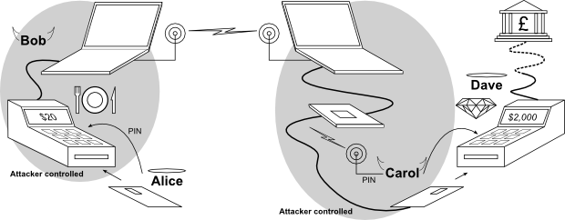 |
We use the mafia-fraud scenario, illustrated in fig:relay_attack, where an unsuspecting restaurant patron, Alice, inserts her smartcard into a terminal in order to pay a 20 charge, which is presented to her on the display.
The terminal looks just like any one of the numerous types of terminals she has used in the past.
This particular terminal, however, has had its original circuitry replaced by the waiter, Bob, and instead of being connected to the bank, it is connected to a laptop placed behind the counter.
As Alice inserts her card into the counterfeit terminal, Bob sends a message to his accomplice, Carol, who is about to pay 2000 for a diamond ring at Dave's jewellery shop.
Carol inserts a counterfeit card into Dave's terminal, which looks legitimate to Dave, but conceals a wire connected to a laptop in her backpack.
Bob and Carol's laptops are communicating wirelessly using mobile-phones or some other network.
The data to and from Dave's terminal is relayed to the restaurant's counterfeit terminal such that the diamond purchasing transaction is placed on Alice's card.
The PIN entered by Alice is recorded by the counterfeit terminal and is sent, via a laptop and wireless headset, to Carol who enters it into the genuine terminal when asked.
When the transaction is over, the crooks have paid for a diamond ring using Alice's money, who got her meal for free, but will be surprised when her bank statement arrives.
Despite the theoretical risk being documented, EMV is vulnerable to the relay attack, as suggested by Anderson et al. [4].
Some believed that engineering difficulties in deployment would make the attack too expensive, or even impossible.
The following section will show that equipment to implement the attack is readily available, and costs are within the expected returns of fraud.
This section describes the equipment we used for implementing the relay attack.
We chose off-the-shelf components that allowed for fast development rather than miniaturisation or cost-effectiveness.
The performance requirements were modest, with the only strict restriction being that our circuit hardware fit within the terminal.
Figure 2:
Photographs of tampered terminal and counterfeit card.
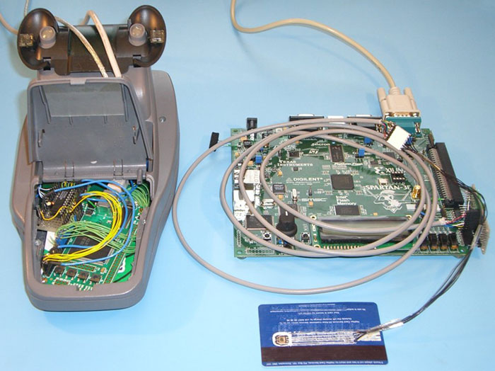
With the exterior intact, the terminal's
original internal circuitry was replaced by a small factor FPGA board (left);
FPGA based smartcard emulator (right) connected to counterfeit card (front)
Customer's view of terminal playing Tetris
|
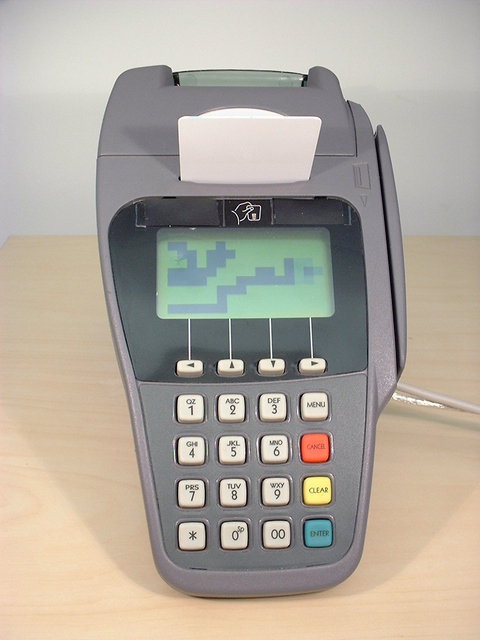
Chip & PIN terminals are readily available for purchase online and their sale is not restricted.
While some are as cheap as 10, our terminal was obtained for 50 from eBay and was ideal for our purposes due to its copious internal space.
Even if second hand terminals were not so readily available, a plausible counterfeit could be made from scratch as it is only necessary that it appears legitimate to untrained customers.
Instead of reverse engineering the existing circuit, we stripped all internal hardware except for the keypad and LCD screen, and replaced it with a 200 Xilinx Spartan-3 small factor, USB-controlled, development board.
We also kept the original smartcard reader slot, but wired its connections to a 40 USB GemPC Twin reader so we could connect it to the laptop.
The result is a terminal with which we can record keypad strokes, display content on the screen and interact with the inserted smartcard.
The terminal appears and behaves just like a genuine one to the customer even though it lacks the ability to communicate with the bank.
At the jeweller's, Carol needs to insert a counterfeit card connected to her laptop, into Dave's terminal.
We took a genuine Chip & PIN card and ground down the resin-covered wire bonds that connect the chip to the back of the card's pads.
With the reverse of the pads exposed, using a soldering iron, we pressed into the plastic thin, flat wires to the edge of the card.
This resulted in a card that looked authentic from on the top side, but was actually wired on the back side, as shown in fig:fakecard.
The counterfeit card was then connected through a 1.5 m cable to a 150 Xilinx Spartan-3E FPGA Starter Kit board to buffer the communications and translate them between the ISO 7816 and RS-232 protocols.
Since the FPGA is not 5V tolerant, we use 390 resistors on the channels that receive data from the card. For the bi-directional I/O channel, we use the Maxim 1740/1 level translator, which costs less than 2. resistors on the channels that receive data from the card. For the bi-directional I/O channel, we use the Maxim 1740/1 level translator, which costs less than 2.
The counterfeit terminal and card are controlled by separate laptops via USB and RS-232 interfaces, respectively, using custom software written in Python.
The laptops communicate via TCP over 802.11b wireless, although in principle this could be GSM or other wireless protocol.
This introduces significant latency, but far less than would be a problem as the timing critical operations on the counterfeit card are performed by the FPGA with real-time guarantees.
One complication of selecting an off-the-shelf USB smartcard reader for the counterfeit terminal is that it operates at the application protocol data unit (APDU) level and buffers an entire command or response before sending it to the smartcard or the PC.
This increases the time between when the genuine terminal sends a command and when the response can be sent; but, as previously mentioned, this is well within tolerances.
This paper only deals with the ``T=0'' ISO 7816 sub-protocol, as used by all EMV smartcards we have examined.
Here, commands are uni-directional, i.e. either the command or response contains a payload but not both.
Upon receiving a command code from the genuine terminal, any associated payload will not be sent by the terminal until the card acknowledges the command. The counterfeit card thus cannot tell whether to request a payload (for terminal  card commands) or send the command code to the genuine card immediately (for card terminal commands). card commands) or send the command code to the genuine card immediately (for card terminal commands).
Were the counterfeit terminal to incorporate a character level card reader, the partial command code could be sent to the genuine card and the result examined to determine the direction, but this is not permissible for APDU level transactions.
Hence, the controlling software must be told the direction for each of the 14 command codes.
Other than this detail, the relay attack is protocol-agnostic and could be deployed against any ISO 7816 based system.
EMV offers a large variety of options, but the generality of the relay attack allows our implementation to account for them all; for simplicity, we will describe the procedure for the common case in the UK.
That is, SDA card authentication (only the static cryptographic signature of the card details is checked), online transaction authorization (the merchant will connect to the issuer to verify that adequate funds are available) and offline plaintext PIN cardholder verification (the PIN entered by the cardholder is sent to the card, unencrypted, and the card will check its correctness).
Transaction authorization is accomplished by the card generating an application cryptogram (AC), which is authenticated by the card's symmetric key and incorporates transaction details from the terminal, a card transaction counter, and whether the PIN was entered correctly.
Thus, the issuing bank can confirm that the genuine card was available and the correct PIN was used. Note that this only requires symmetric cryptography, and so will work even with SDA-only cards, as issued in the UK.
The protocol can be described in six steps:
- Initialization:
- The card is powered up and returns the ATR. Then the terminal selects one of the possible payment applications offered by the card.
- Read application data
- The terminal requests card details (account number, name, expiration date etc.) and verifies the static signature.
- Cardholder verification:
- The cardholder enters their PIN into the merchant's terminal and this is sent to the card for verification. If correct, the card returns a success code, otherwise the cardholder may try again until the maximum number of PIN attempts have been exceeded.
- Generate AC 1:
- The terminal requests an authorization request cryptogram (ARQC) from the card, which is sent to the issuing bank for verification, which then responds with the issuer authentication data.
- External authenticate:
- The terminal sends the issuer authentication data to the card.
- Generate AC 2:
- The terminal asks the card for a transaction certificate (TC) which the card returns to the terminal if, based on the issuer authentication data and other internal state, the transaction is approved. Otherwise, it returns an application authentication cryptogram (AAC), signifying the transaction was denied. The TC is recorded by the merchant to demonstrate that it should receive the funds.
This flow imposes some constraints on the relay attack. Firstly, Alice must insert her card before Carol inserts her counterfeit card in order for initialization and read application data to be performed.
Secondly, Alice must enter her PIN before Carol is required to enter it into the genuine terminal.
Thirdly, Alice must not remove her card until the Generate AC 2 stage has occurred.
Thus, the two sides of the radio link must be synchronised, but there is significant leeway as Carol can stall until she receives the signal to insert her card.
After that point, the counterfeit card can request extra time from the terminal, before sending the first response, by sending a null procedure byte (0x60).
The counterfeit terminal can also delay Alice by pretending to dial-up the bank and waiting for authorization until Carol's transaction is complete.
All timing critical sections, such as sending the ATR in response to de-assertion of reset and the encoding/decoding of bytes sent on the I/O, are implemented on the FPGA to ensure a fast enough response.
There are wide timing margins between the command and response, so this is managed in software.
We tested our relay setup with a number of different smartcard readers in order to test its robustness.
Firstly, we used a VASCO Chip Authentication Program (CAP) reader (a similar device, but manufactured by Gemalto, is marketed by the UK bank Barclays as PINsentry).
This is a handheld one-time-password generator for use in online banking, and implements a subset of the EMV protocol.
Specifically, it performs cardholder verification by checking the PIN and requests an application cryptogram, which may be validated online.
Our relay setup was able to reliably complete transactions, even when we introduced an extra three seconds of latency between command and response.
While the attack we describe in most detail uses the counterfeit card in a retail outlet, a fraudster could equally use a CAP reader to access the victim's online banking.
This assumes that the PIN used for CAP is the same as for retail transactions and the criminal knows all other login credentials.
The CAP reader uses a 1MHz clock to decrease power consumption, but at the cost of slower transactions.
We also tested our relay setup with a GemPC Twin reader, which operates at a 4MHz frequency. The card reader was controlled by our own software, which simulates a Chip & PIN transaction.
Here, the relay device also worked without any problems and results were identical to when the card was connected directly to the reader.
Finally, we developed a portable version of the equipment, and took this to a merchant with a live Chip & PIN terminal.
With the consent of the merchant and cardholder, we placed a transaction with our counterfeit card in the genuine terminal, and the cardholder's card in the counterfeit terminal.
In addition to the commands and responses being relayed, the counterfeit terminal was connected to a laptop which, through voice-synthesis software, read out the PIN to our ``Carol''.
The transaction was completed successfully.
One such demonstration of our equipment was shown on the UK consumer rights programme BBC Watchdog on 6th February 2007.
The relay attack is also applicable where ``Alice'' is not the legitimate card holder, but a thief who has stolen the card and observed the PIN.
To frustrate legal investigation and fraud detection measures, criminals commonly use cards in a different country from where they were stolen.
Magnetic stripe cards are convenient to use in this way, as the data can be read and sent overseas, to be written on to counterfeit cards.
However, chip cards cannot be fully duplicated, so the physical card would need to be mailed, introducing a time window where the cardholder may report the card stolen or lost.
The relay attack can allow fraudsters to avoid this delay by making the card available online using a card reader and a computer connected to the Internet.
The fraudster's accomplice in another country could connect to the card remotely and place transactions with a counterfeit one locally.
The timing constraints in this scenario are more relaxed as there is no customer expecting to remove their genuine card.
Finally, in certain types of transactions, primarily with unattended terminals, the PIN may not be required, making this attack easier still.
APACS, the UK payment association, say they are unaware of any cases of relay attacks being used against Chip & PIN in the UK [5].
The reason, we believe, is that even though the cost and the technical expertise that are required for implementing the attack are relatively low, there are easier ways to defeat the system.
Methods such as card counterfeiting/theft, mail interception, and cardholder impersonation are routinely reported and are more flexible in deployment.
These security holes are gradually being closed, but card fraud remains a lucrative industry - in 2006 £428m ( 850m) of fraud was suffered by UK banks [6].
Criminals will adapt to the new environment and, to maintain their income, will likely resort to more technically demanding methods, so now is the time to consider how to prevent relay attacks for when that time arrives. 850m) of fraud was suffered by UK banks [6].
Criminals will adapt to the new environment and, to maintain their income, will likely resort to more technically demanding methods, so now is the time to consider how to prevent relay attacks for when that time arrives.
4 Defences
The previous section described how feasible it is to deploy relay attacks against Chip & PIN and other smartcard based authorization systems in practice.
Thus, system designers must develop mitigation techniques while, for economic consideration, staying within the deployed EMV framework as much as possible.
4.1 Non-solutions
In this section we describe a number of solutions that are possible, or have been proposed, against our attack and assess their overall effectiveness.
A pre-requisite of our relay attack is that Alice will insert her card and enter her PIN into a terminal that relays these details to the remote attacker.
The terminal, therefore, must either be tampered with or be completely counterfeit, but still acceptable to cardholders.
This implies a potential solution - allow the cardholder to detect malicious terminals so they will refuse to use them.
Unfortunately, this cannot be reliably done in practice.
Although terminals do implement internal tamper-responsive measures, when triggered, they only delete keys and other data without leaving visible evidence to the cardholder.
Tamper-resistant seals could be inspected by customers, but Johnston et al. [21] have shown that many types of seals can be trivially bypassed.
It would also be infeasible to give all customers adequate training to detect tampering or counterfeiting of seals.
By inducing time-pressure and an awkward physical placement of the terminal, the attacker can make it extremely difficult for even a diligent customer to check for tampering.
Even if it was possible to produce an effective seal, there are, as of May 2007, 304 VISA approved terminal designs from 88 vendors [24], so cardholders cannot be expected to identify them all.
Were there only one terminal design, the use of counterfeit terminals would have to be prevented, which raises the same problems as tamper-resistant seals.
Finally, with the large sums of money netted by criminals from card fraud, fabricating plastic parts is well within their budget.
While relay attacks will induce extra delays between commands being sent by the terminal and responses being received, existing smartcard systems are tolerant to very high latencies.
We have successfully tested our relay device after introducing a three second delay into transactions, in addition to the inherent delay of our design.
This extra round-trip time could be exploited by an attacker 450000km away, assuming that signals propagate at the speed of light.
Perhaps, then, attacks could be prevented by requiring that cards reply to commands precisely after a fixed delay.
Terminals could then confirm that a card responds to commands promptly and will otherwise reject a transaction.
Other than the generate AC command, which includes a terminal nonce, the terminal's behaviour is very predictable.
So an attacker could preemptively request these details from the genuine card then send them to the counterfeit card where they are buffered for quick response.
Thus, the value of latency as a distance measure can only be exploited at the generate AC stages.
Furthermore, Clulow et al. [12] show how wireless distance bounding protocols, based on channels which were not designed for the purpose, can be circumvented. Their comments apply equally well to wired protocols such as ISO 7816.
To hide the latency introduced by mounting the relay attack, the attacker aims to sample signals early and send signals late, while still maintaining their accuracy.
In ISO 7816, cards and terminals are required to sample the signal between the 20% and 80% portion of the bit-time and aim to sample at the 50% point.
However, an attacker with sensitive equipment could sample near the beginning, and send their bit late. The attacker then gains 50% of a bit-width in both directions, which at a 5MHz clock is 37
 , or 11km. , or 11km.
The attacker could also over-clock the genuine card so the responses are returned more quickly.
A DES calculation could take around 100ms so only a 1% increase would give a 300km distance advantage.
Even if the calculation time was fixed, and only receiving the response from the card could be accelerated, the counterfeit card could preemptively reply with the predictable 11 bytes (2 byte response code, 5 byte read more command, 2 byte header and 2 byte counter) each taking 12 bit-widths (start, 8 data bits, stop and 2 bits guard time).
At
 this gives the attacker 98
, i.e. 29km. this gives the attacker 98
, i.e. 29km.
One EMV-specific problem is that the contents of the payload in the generate AC command are specified by the card in the card risk management data object list (CDOL).
Although the terminal nonce should be at the end of the message in order to achieve maximum resistance to relay attacks, if the CDOL is not signed, the attacker could substitute the CDOL for one requesting the challenge near the beginning.
Upon receiving the challenge from the terminal, the attacker can then send this to the genuine card.
Other than the nonce, the rest of the generate AC payload is predictable, so the counterfeit terminal can restore the challenge to the correct place, fill in the other fields and send it to the genuine card.
Thus, the genuine card will send the correct response, even before the terminal thinks it has finished sending the command.
A payload will be roughly 30 bytes, which at 5MHz gives 27ms and a 8035km distance advantage.
Nevertheless, eliminating needless tolerance to response latency would decrease the options available to the attacker.
If it were possible to roll out this modification to terminals as a software upgrade, it might be expedient to plan for this alteration to be quickly deployed in reaction to actual use of the relay attack.
While we have described how this countermeasure could be circumvented, attackers who build and test their system with high latency would be forced to re-architect it if the acceptable latency of deployed terminals were decreased without warning.
4.2 Procedural improvements
Today, merchants and till operators are accustomed to looking away while customers enter their PIN and seldom handle the card at all, while customers are often recommended not to allow anyone but themselves to handle the card because of card skimming.
In the case of relay attacks, this assists the criminal, not the honest customer or merchant.
If the merchant examined the card, even superficially, he would detect the relay attack, as we implemented it, by spotting the wires.
That said, it is not infeasible that an RFID proximity card could be modified to relay data wirelessly to a local receiver and therefore appear to be a genuine one.
A stronger level of protection can be achieved if, after the transaction is complete, the merchant checks not only that the card presented is legitimate, but also that the embossed card number matches the one on the receipt.
In the case of the relay attack, the receipt will show the victim's card number, whereas the counterfeit card will show the original number of the card from before it was tampered.
For these to match, the fraudster must have appropriate blank cards and an embossing machine, in addition to knowing the victim's card number in advance.
Alternatively, a close to real-time attack could still be executed with a portable embossing machine.
Existing devices take only a few seconds to print a card and it is feasible that fraudsters can make them portable.
The quality of counterfeit cards and embossing need not be high, just sufficient to pass a cursory inspection.
More recent smartcards are being issued without embossing, as the carbon-paper payment method is no longer used, making counterfeits even easier to produce.
If none of these possibilities are open to the fraudster, repeat customers could be targeted and so creating a wide window of opportunity.
In some scenarios, such as unattended Chip & PIN terminals, ATMs, or where the terminal is on the opposite side of a glass barrier, physical card inspections would not be possible; but even where it is, the merchant must be diligent.
Varian [23] argues that if the party who is in the best position to prevent fraud does not have adequate incentives to do so, security suffers.
If customers must depend on merchants, who they have no relationship with, for their protection, then there are mismatched incentives.
Merchants selling low-marginal-cost products or services (e.g. software or multimedia content), have little desire to carefully check for relay attacks. This is because, in the case of fraud, costs will likely be borne by the customer.
Even if the transaction is subsequently reversed when fraud is detected, the merchant has lost only the low marginal cost and the chargeback overhead, but has saved the effort of checking cards.
4.3 Hardware alterations
The electronic attorney is a trusted device that is brought into the transaction by the customer so that the merchant's terminal does not need to be trusted; this is called the ``man-in-the-middle defence'', as suggested by Anderson and Bond [2]; trusted devices to protect customers are also discussed by Asokan et al. [7].
The device is inserted into the terminal's card slot while the customer inserts their card into the device.
The device can display the transaction value as it is parsed from the data sent from the terminal, allowing the customer to verify that she is charged the expected amount.
If the customer approves the transaction, she presses a button on the electronic attorney itself, which allows the protocol to proceed.
This trusted user interface is necessary, since if a PIN was used as normal, a fraudster could place a legitimate transaction first, which is accepted by the customer, but with knowledge of the PIN a subsequent fraudulent one can be placed.
Alternatively, one-time-PINs could be used, but at a cost in usability.
Because the cardholder controls the electronic attorney, and it protects the cardholder's interests, the incentives are properly aligned.
Market forces in the business of producing and selling these devices should encourage security improvements.
However, this extra device will increase costs, increase complexity and may not be approved of by banking organizations.
Additionally, fraudsters may attempt to discourage their use, either explicitly or by arranging the card slot so the use of a electronic attorney is difficult.
A variant of the trusted user interface is to integrate a display into the card itself [8].
Another realization of the trusted user interface for payment applications is to integrate the functionality of a smartcard into the customer's mobile phone.
This can allow communication with the merchant's terminal using near field communications (NFC) [20].
This approach is already under development and has the advantage of being a customer-controlled device with a large screen and convenient keypad, allowing the merchant's name and transaction value to be shown and once authorized by the user, entry of the PIN.
Wireless communications also ease the risk of a malicious merchant arranging the terminal so that the trusted display device is not visible.
Although mobile phones are affordable and ubiquitous, they may still not be secure enough for payment applications as they can be, for example, targeted by malware.
5 Distance bounding
None of the techniques detailed in sec:nonsolutions are adequate to completely defeat relay attacks.
They are either impractical (tamper-resistant terminals), expensive (adding extra hardware) or circumventable (introducing tighter timing constraints and requiring merchants to check card numbers).
Due to the lack of a customer-trusted user interface on the card, there is no way to detect a mismatch between the data displayed on the terminal and the data authorized by the card.
However, relay attacks can be foiled if either party can securely establish the position of the card which is authorizing the transaction, relative to the terminal processing it.
Absolute positioning is infeasible due to the cost and form factor requirements of smartcards being incompatible with GPS, and also because the civilian version is not resistant to spoofing [22].
However, it is possible for the terminal to securely establish a maximum distance bound, by measuring the round-trip-time between it and the smartcard; if this time is too long, an alarm would be triggered and the transaction refused.
Despite the check being performed at the merchant end, the incentive-compatibility problem is lessened because the distance verification is performed by the terminal and does not depend on the sales assistant being diligent.
The approach of preventing relay attacks by measuring round-trip-time was first proposed by Beth and Desmedt [9] but Brands and Chaum [11] described the first concrete protocol.
The cryptographic exchange in our proposal is based on the Hancke-Kuhn protocol [17], because it requires fewer steps, and it is more efficient if there are transmission bit errors compared to Brands-Chaum.
However, the Hancke-Kuhn protocol is proposed for ultra-wideband radio (UWB), whereas we require synchronous half-duplex wired transmission.
One characteristic of distance-bounding protocols, unlike most others, is that the physical transmission layer is security-critical and tightly bound to the other layers, so care must be taken when changing the transmission medium.
Wired transmission introduces some differences, which must be taken into consideration.
Firstly, to avoid circuitry damage or signal corruption, in a wired half duplex transmission, contention (both sides driving the I/O at the same time) must be avoided.
Secondly, whereas UWB only permits the transmission of a pulse, wired allows a signal level to be maintained for an extended period of time.
Hence, we may skip the initial distance-estimation stage of the Hancke-Kuhn setup and simplify our implementation.
While in this section we will describe our implementation in terms of EMV, implemented to be compatible with ISO 7816, it should be applicable to any wired, half-duplex synchronous serial communication line.
In EMV, authentication is only card to terminal so we follow this practise.
Following the Hancke-Kuhn terminology, the smartcard is the prover,  , and terminal is the verifier, , and terminal is the verifier,  .
This is also appropriate because the Hancke-Kuhn protocol puts more complexity in the verifier than the prover, and terminals are several orders of magnitude more expensive and capable than the cards.
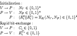
The protocol is described as follows: .
This is also appropriate because the Hancke-Kuhn protocol puts more complexity in the verifier than the prover, and terminals are several orders of magnitude more expensive and capable than the cards.
The protocol is described as follows:
At the start of the initialization phase, nonces and parameters are exchanged over a reliable data channel, with timing not being critical.
 and and  provide freshness to the transaction in order to prevent replay attacks, with the latter preventing a middle-man from running the complete protocol twice between the two phases using the same and complementary provide freshness to the transaction in order to prevent replay attacks, with the latter preventing a middle-man from running the complete protocol twice between the two phases using the same and complementary  and thus, obtain both and thus, obtain both  and and  .
The prover produces a MAC under its key, .
The prover produces a MAC under its key,  , using a keyed pseudo-random function, the result of which is split into two shift registers, and . , using a keyed pseudo-random function, the result of which is split into two shift registers, and .
In the timing-critical rapid bit-exchange phase, the maximum distance between the two participants is determined.
sends a cryptographically secure pseudorandom single-bit challenge to , which in turn immediately responds with  , the next single-bit response, from the corresponding shift register.
A transaction of a 32 bit exchange is shown in tab:transaction. , the next single-bit response, from the corresponding shift register.
A transaction of a 32 bit exchange is shown in tab:transaction.
Table 1:
Example of the rapid bit-exchange phase of the distance bounding protocol.
For clarity,  is shown instead of the response bits not sent by the prover.
The left most bit is sent first. is shown instead of the response bits not sent by the prover.
The left most bit is sent first.
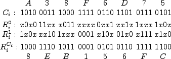 |
If a symmetric key is used, this will require an on-line transaction to verify the result because the terminal does not store .
If the card has a private/public key pair, a session key can be established and the final challenge-response can also be verified offline.
The values  and and  , the nonce and shift register bit lengths, respectively, are security parameters that are set according to the application and are further discussed in sec:attacks. , the nonce and shift register bit lengths, respectively, are security parameters that are set according to the application and are further discussed in sec:attacks.
This exchange succeeds in measuring distance because it necessitates that a response bit arrive at a certain time after the challenge has been sent.
When the protocol execution is complete, 's response register, , is verified by the terminal or bank to determine if the prover is within the allowed distance for the transaction.
ISO 7816, our target application, dictates that the smartcard (prover) is a low resource device, and therefore, should have minimal additions in order to keep costs down; this was our prime constraint.
The terminal (verifier), on the other hand, is a capable, expensive device that can accommodate moderate changes and additions without adversely affecting its cost.
Of course, the scheme must be secure to all attacks devised by a highly capable adversary that can relay signals at the speed of light, is able to ensure perfect signal integrity, and can clock the smartcard at higher frequencies than it was designed for.
We assume, however, that this attacker does not have access to the internal operation of the terminal and that extracting secret material out of the smartcard, or interfering with its security critical functionality, is not economical considering the returns from the fraud.
Table 2:
Signals and their associated timing parameters.
|
Figure 3:
Waveforms of a single bit-exchange of the distance bounding protocol.
 is the verifier's clock; is the verifier's clock;
 drives the challenge on to I/O; drives the challenge on to I/O;
 samples the response; samples the response;
 is the prover's clock; is the prover's clock;
 and and
 are versions of the I/O on each side accounting for the propagation delay are versions of the I/O on each side accounting for the propagation delay  ; ;
 is the received clock that is used to sample the challenge; and is the received clock that is used to sample the challenge; and
 drives the response on to the I/O. drives the response on to the I/O.
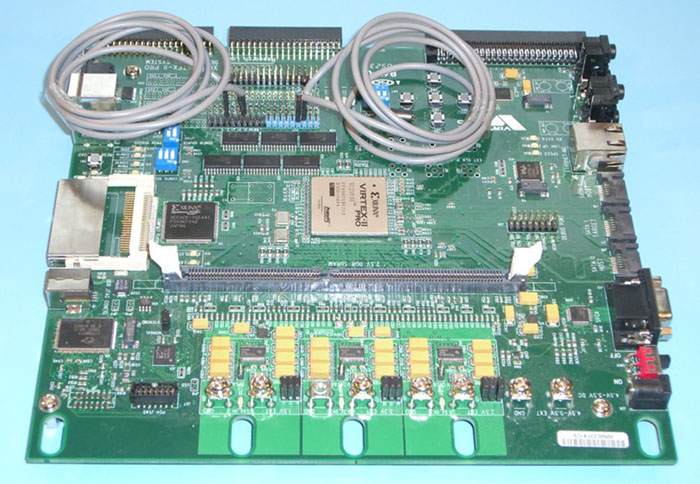 |
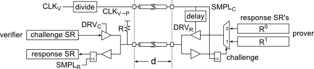
Figure 4:
Simplified diagram of the distance bounding circuit.
controls when the challenge is put on the I/O line.
 controls the verifier's circuit; it is divided and is received as
at the prover where it is used to sample the challenge.
A delay element produces
, which controls when the response is put the I/O, while at the verifier
samples it.
The pull-up resistor controls the verifier's circuit; it is divided and is received as
at the prover where it is used to sample the challenge.
A delay element produces
, which controls when the response is put the I/O, while at the verifier
samples it.
The pull-up resistor  is present to pull the I/O line to a stable state when it is not actively driven by either side. is present to pull the I/O line to a stable state when it is not actively driven by either side.
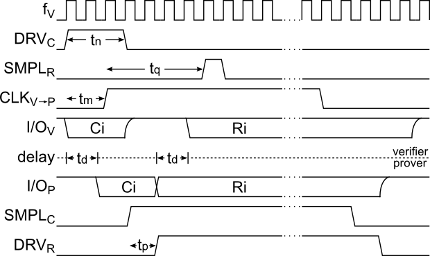 |
For this section refer to tab:signals for signal names and their function, fig:circuit for the circuit diagram and fig:waveform for the signal waveforms.
As opposed to the prover, the verifier may operate at high frequencies.
We have implemented the protocol such that one clock cycle of the verifier's operating frequency, , determines the distance resolution.
Since signals cannot travel faster than the speed of light,  , the upper-bound distance resolution is therefore, , the upper-bound distance resolution is therefore,  .
Thus, , should be chosen to be as high as possible.
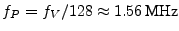
We selected 200 MHz which allows us a 1.5m resolution under ideal conditions for the attacker.
We have made the prover's operating frequency, .
Thus, , should be chosen to be as high as possible.
We selected 200 MHz which allows us a 1.5m resolution under ideal conditions for the attacker.
We have made the prover's operating frequency,  , compatible with any frequencies having a high-time greater than , compatible with any frequencies having a high-time greater than
 , where , where  defines the time between when the challenge is being driven onto the I/O and when the response is sampled by the verifier; is the delay between and .
ISO 7816 specifies that the smartcard/prover needs to operate at 1-5 MHz and in order to be compatible, we chose defines the time between when the challenge is being driven onto the I/O and when the response is sampled by the verifier; is the delay between and .
ISO 7816 specifies that the smartcard/prover needs to operate at 1-5 MHz and in order to be compatible, we chose
 for our implementation. for our implementation.
The design has four 64 bit shift registers (SR): the verifier's challenge and received response SR's and the prover's two response SR's.
The challenge SR is clocked by
and is shifted one clock cycle before it is driven on to the I/O line by
.
The verifier's response SR is also clocked by
and is shifted on the rising edge of
.
On the prover side, the SR's are clocked and shifted by
.
The verifier and prover communicate using a bi-directional I/O with tri-state buffers at each end.
These buffers are controlled by the signals
and
and are implemented such that only one side drives the I/O line at any given time in order to prevent contention.
This is a consequence of adapting the Hancke-Kuhn protocol to a wired medium, and implies that the duration of the challenge must be no longer than necessary, so as to obtain the most accurate distance bound.
A pull-up is also present, as with the ISO 7816 specification, to maintain a high state when the line is not driven by either side.
As a side note, if the constraints imposed by ISO 7816 are not to be adhered to, two uni-directional wires for the challenge and response could have been used for easier implementation.
A timing diagram of a single challenge-response exchange is shown in fig:waveform.
The circuit shown in fig:circuit was implemented on an FPGA using Verilog (not all peripheral control signals are shown for the sake of clarity).
Since we used a single chip, the I/O and clock lines were ``looped-back'' using various length transmission wires to simulate the distance between the verifier and prover as shown in fig:xup.
Figure 5:
The Xilinx XUP board with a VirtexII-PRO 30 FPGA on which the distance bounding design was implemented.
Both verifier and prover reside on the same chip connected only by two same-length tranmission lines for I/O and clock (1m shielded cables are shown).
 |
The first operation is clocking the challenge shift register (not shown), which is driven on to the I/O line by
on the following clock cycle for a  period.
should be made long enough to ensure that the prover can adequately and reliably sample the challenge, and as short as possible to allow the response to be rapidly sent while not causing contention.
The clock sent to ,
, is asserted period.
should be made long enough to ensure that the prover can adequately and reliably sample the challenge, and as short as possible to allow the response to be rapidly sent while not causing contention.
The clock sent to ,
, is asserted  after the rising edge of
.
Both
and the I/O line have the same propagation delay, , and when the clock edge arrives (now called
), it samples the challenge.
The same clock edge also shifts the two response registers, one of which is chosen by a 2:1 multiplexer that is controlled by the sampled challenge. after the rising edge of
.
Both
and the I/O line have the same propagation delay, , and when the clock edge arrives (now called
), it samples the challenge.
The same clock edge also shifts the two response registers, one of which is chosen by a 2:1 multiplexer that is controlled by the sampled challenge.
 is a delayed replica of
, which is created using a delay element. is a delayed replica of
, which is created using a delay element.
The delay,  , allows the response SR signals to shift and propagate through the multiplexer, preventing the intermediate state of the multiplexer from being leaked.
Otherwise, the attacker could discover both responses to the previous challenge in the case where , allows the response SR signals to shift and propagate through the multiplexer, preventing the intermediate state of the multiplexer from being leaked.
Otherwise, the attacker could discover both responses to the previous challenge in the case where
 .
may be very short but should be at least as long as the period from the rising edge of
to when the response emerges from the multiplexer's output; in our implementation, we used deliberately placed routing delays to adjust , which can be as short as 500ps.
When
is asserted, the response is being driven on to the I/O line until the falling edge. .
may be very short but should be at least as long as the period from the rising edge of
to when the response emerges from the multiplexer's output; in our implementation, we used deliberately placed routing delays to adjust , which can be as short as 500ps.
When
is asserted, the response is being driven on to the I/O line until the falling edge.
At the verifier, the response is sampled by
after from the assertion of
.
The value of determines the distance measured and should be long enough to account for the propagation delay that the system was designed for (including on-chip and package delays), and short enough to not allow an attacker to be further away than desired, with the minimum value being
 .
As an improvement, can be dynamically adjusted between invocations of the protocol allowing the verifier to make decisions based on the measured distance, for example, determine the maximum transaction amount allowed.
With a single iteration, the verifier can discover the prover's maximum distance away, but with multiple iterations, the exact distance can be found with a margin of error equal to the signal propagation time during a single clock cycle of the verifier.
may be made to sample on both rising and falling edges of , effectively doubling the distance resolution without increasing the frequency of operation (other signals may operate this way for tighter timing margins). .
As an improvement, can be dynamically adjusted between invocations of the protocol allowing the verifier to make decisions based on the measured distance, for example, determine the maximum transaction amount allowed.
With a single iteration, the verifier can discover the prover's maximum distance away, but with multiple iterations, the exact distance can be found with a margin of error equal to the signal propagation time during a single clock cycle of the verifier.
may be made to sample on both rising and falling edges of , effectively doubling the distance resolution without increasing the frequency of operation (other signals may operate this way for tighter timing margins).
If we assume that an attacker can transmit signals at the speed of light and ignore the real-life implications of sending them over long distances, we can determine the theoretical maximum distance between the verifier and prover.
A more realistic attacker will need to overcome signal integrity issues that are inherent to any system.
We should not, therefore, make it easy for the attacker by designing with liberal timing constraints, and choose the distance between the verifier and prover,  , to be as short as possible.
More importantly, we should carefully design the system to work for that particular distance with very tight margins.
For example, the various terminals we have tested were able to transmit/drive a signal through a two meter cable, although the card should at most be a few centimeters away.
Weak I/O drivers could be used to degrade the signal when an extention is applied.
The value of also determines most of the timing parameters of the design, and as we shall see next, the smaller these are, the harder it will be for the attacker to gain an advantage. , to be as short as possible.
More importantly, we should carefully design the system to work for that particular distance with very tight margins.
For example, the various terminals we have tested were able to transmit/drive a signal through a two meter cable, although the card should at most be a few centimeters away.
Weak I/O drivers could be used to degrade the signal when an extention is applied.
The value of also determines most of the timing parameters of the design, and as we shall see next, the smaller these are, the harder it will be for the attacker to gain an advantage.
5.5 Possible attacks on distance bounding
Although, following from our previous assumptions, the attacker cannot get access to any more than half the response bits, there are ways he may extend the distance limit before a terminal will detect the relay attack. This section discusses which options are available, and their effectiveness in evading defences.
Following the initialization phase, the attacker can initiate the bit-exchange phase before the genuine terminal has done so.
As the attacker does not know the challenge at this stage, he will, on average, guess 50% of the challenge bits correctly and so receive the correct response for those.
For the ones where the challenge was guessed incorrectly, the response is effectively random, so there is still a 50% chance that the response will be correct.
Therefore the expected success rate of this technique is 75%.
Since our tests show a negligible error rate, the terminal may reject any response with a single bit that is incorrect.
In our prototype, where the response registers are 64 bits each, the attacker will succeed with probability
 .
The size of the registers is a security parameter that can be increased according to the application, while the nonces assure that the attacker can only guess once. .
The size of the registers is a security parameter that can be increased according to the application, while the nonces assure that the attacker can only guess once.
If the attacker can force the card to perform two protocol runs, with the same nonces used for both, then all bits of the response can be extracted by sending all 1's on the first iteration and all 0's on the second.
We resist this attack by selecting the protocol variant mentioned by Hancke and Kuhn [17], where the card adds its own nonce.
This is cheap to do within EMV since a transaction counter is already required by the rest of the protocol.
If this is not desired then provided the card cannot be clocked at twice its intended frequency, the attacker will not be able to extract all bits in time.
This assumes that the time between starting the distance bounding protocol, and the earliest time the high-speed stage can start, is greater than the latter's duration.
The card will not sample the terminal's challenge until  after the challenge is placed on the I/O line.
This is to allow an inexpensive card to reliably detect the signal but, as Clulow et al. [12] suggest, an attacker who is willing to invest in expensive equipment could, in theory, detect the signal immediately.
By manipulating the clock provided to the genuine card, and using high-quality signal drivers, the challenge could be sent to the card with less of a delay. after the challenge is placed on the I/O line.
This is to allow an inexpensive card to reliably detect the signal but, as Clulow et al. [12] suggest, an attacker who is willing to invest in expensive equipment could, in theory, detect the signal immediately.
By manipulating the clock provided to the genuine card, and using high-quality signal drivers, the challenge could be sent to the card with less of a delay.
Similarly, the terminal will wait between sending the challenge and sampling the response, to allow for the round trip signal propagation time, and wait until the response signal has stabilized.
Again, with superior equipment the response could be sent from the card just before the terminal samples.
The attacker, however, cannot do so any earlier than after the card has sampled the challenge, and the response appears on the I/O.
The card may include the value of in its signed data, so the attacker cannot make the terminal believe that the value is larger than the card's specification.
However, the attacker might be able to reduce the delay, for example by cooling the card.
If it can be reduced to the point that the multiplexer or latch has not settled, then both potential responses may be placed on to the I/O line, violating our assumptions.
However, if the circuit is arranged so that the delay will be reduced only if the reaction of the challenge latch and multiplexer is improved accordingly, the response will still be sent out prematurely.
This gives the attacker extra time, so should be prevented.
If temperature compensated delay lines are not economic, then they should be as short as possible to reduce this effect.
In fact, may be so small, even less than 1ns, that the terminal could just assume it would be zero.
This will mean that the terminal will believe all cards are slightly further away than they really are, but will avoid the value of having to be included in the signed data.
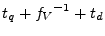
For an attacker to gain a better than  in in  probability of succeeding in the challenge response protocol, the relay attack must take less than probability of succeeding in the challenge response protocol, the relay attack must take less than  time.
In practice, an attacker will not be able to sample or drive the I/O line instantaneously and the radio-link transceiver or long wires will introduce latency, so the attacker would need to be much closer than this limit.
A production implementation on an ASIC would be able to give better security guarantees and be designed to tighter specifications than were available on the FPGA for our prototype. time.
In practice, an attacker will not be able to sample or drive the I/O line instantaneously and the radio-link transceiver or long wires will introduce latency, so the attacker would need to be much closer than this limit.
A production implementation on an ASIC would be able to give better security guarantees and be designed to tighter specifications than were available on the FPGA for our prototype.
We have developed a versatile implementation that requires only modest modification to currently deployed designs.
Our distance bounding scheme was successfully implemented and tested on an FPGA for 2.0, 1.0, and 0.3 meter transmission lengths, although it can be modified to work for any distance and tailored to any end application.
Oscilloscope traces of a single bit challenge-response exchange over a 50, 30cm printed circuit board transmission line are shown in fig:trace.
In this case, the challenge is 1 and the response is 0 with indicators where
has sampled the response.
The first, after
 has sampled too early while the second, has sampled too early while the second,
 , which is a single period of later, has correctly sampled the 0 as the response.
The delay , which is a single period of later, has correctly sampled the 0 as the response.
The delay
 , can also be seen and is, of course, due to the length of the transmission line.
If the attacker exploited all possible attacks previously discussed and was able to transmit signals at , he would need to be within approximately 6m, although the actual distance would be shorter for a realistic attacker. , can also be seen and is, of course, due to the length of the transmission line.
If the attacker exploited all possible attacks previously discussed and was able to transmit signals at , he would need to be within approximately 6m, although the actual distance would be shorter for a realistic attacker.
The FPGA design of both the verifier and prover as shown in fig:xup consumes 37 flip-flops and 93 look-up tables: 64 for logic, 13 route-throughs, and 16 as shift registers (4 cascaded 16-bit LUTs for each), which is extremely compact, and consumes well under 0.5% of the resources available on our FPGA.
However, it is difficult to estimate the cost of an ASIC implementation with these figures as there is no reliable conversion technique between FPGA resource utilization and ASIC transistor count, especially since the above numbers are for the core functions, without the supporting circuitry.
It is also hard to estimate the cost in currency because that changes rapidly with time, production volume, fabrication process, and many other factors, so we will describe it relative to the resources currently used.
As mentioned, we have made every effort to minimize the circuitry that needs to be added to the smartcard while being more liberal with the terminal, although for both the additions can be considered minor.
For the smartcard, new commands for initiating the initialization phase need to be added as well as two shift registers and a state machine for operating the rapid bit-exchange.
Considering that smartcards already have a few thousand memory cells, this can be considered a minor addition, especially given that they need to operate at the existing low frequencies of 1-5MHz.
For the initialization phase, existing circuits can be used such as the DES engine for producing the content of the response registers.
The card's transaction counter may be used for the nonce,  . .
As for the terminals, their internal operating frequency is unknown to us, but it is unlikely that it is high enough to achieve good distance resolution.
Therefore, a capable processor and some additional components are required, such as a high quality oscillator.
As an alternative to high frequencies, or when designing for very short distances, delay lines could be used instead of operating on clock edges.
The distance bounding circuitry would need to be added to the terminal's main processor, which consists of two shift registers and slightly more involved control code than the smartcard's.
We have described the added cost in terms of hardware but the added time per transaction and the need to communicate with the bank, refused transactions due to failure, re-issuing cards, and so on, may amount to substantial costs. Only the banks involved have access to all the necessary information needed to make a reasonable estimate of these overheads.
6 Discussion
The distance bounding protocol we have proposed will detect attempted relay attacks but requires the banks to produce cards and terminals that support the protocol.
However, the person being defrauded is the cardholder, Alice, who must use the cards and terminals she is given, so has no trusted user interface and no way to protect herself.
As mentioned in sec:procedural, this incentive mismatch may be detrimental to the cardholder's security.
For instance, until all terminals support the distance bounding protocol, the issuer can select whether to fallback to the current protocol that is vulnerable to relay-attacks.
Under existing UK practice, the customer is liable for PIN-verified fraudulent transactions [10], so the issuer may elect to accept fallback transactions knowing that the cardholder is carrying the risk.
A further problem of the distance bounding protocol is the lack of non-repudiation: for a third party to verify that a relay attack was not in progress, the merchant's terminal must be trusted to correctly report the round-trip latency.
Thus, if a customer claims that a transaction is fraudulent, then even if the distance bounding protocol is recorded to have succeeded, there remains the possibility that the terminal has been tampered with.
It falls on the acquirer to mandate tamper-resistant terminals, but although the payment network may require that all members implement appropriate protections, the customer is only represented indirectly by the issuer.
So while inexpensive yet strong technical solutions, such as distance bounding, do exist they must be deployed as part of an appropriate liability framework to fully realize their benefits.
The current situation, where customers are liable for fraud, yet powerless to verify whether a terminal is genuine, is clearly unfair.
If the power of banking institutions is too great to alter the entrenched notion of customer liability, then measures that put the cardholder in a position of control, such as the electronic attorney [2], despite being more expensive, may be the most appropriate solution.
However, customers should exercise caution before accepting these options as the second-order effect of the customer being able to detect attacks could be to make them reasonably liable for any fraud which is nevertheless perpetrated.
This paper described relay attacks and how they can be applied to exploit smartcard-based payment systems.
A prototype was built and shown to be successful against the Chip & PIN payment system deployed in the UK.
This consisted of creating a fake terminal and custom hardware to allow the relaying of information between the participating parties.
We suggested procedural improvements to the acceptance of Chip & PIN transactions, which would provide a short-term defence, but these could be circumvented by a plausible attacker.
We then developed the first implementation of a distance bounding defence against these relay attacks and showed it to be the most robust solution.
Our implementation was designed to be appealing for adoption in the next generation of smartcards by tailoring the design to the EMV framework.
Future work may include implementing a wireless variant of the protocol, mutual distance bound establishment and customizing the system to other applications.
Saar Drimer is funded by Xilinx, Inc.
Steven J. Murdoch is funded by the OpenNet Initiative.
Markus Kuhn has provided us with both stimulating discussions and advice, along with hardware.
Xilinx donated hardware and development software.
We also thank Ross Anderson, Mike Bond, Richard Clayton, Frank Stajano, Robert Watson, Ford-Long Wong, anonymous reviewers for their valuable suggestions, and the merchants who allowed us to test and demonstrate our attack.
- 1
-
ADIDA, B., BOND, M., CLULOW, J., LIN, A., MURDOCH, S. J., ANDERSON, R. J.,
AND RIVEST, R. L.
Phish and chips (traditional and new recipes for attacking EMV).
In Security Protocols Workshop (Cambridge, England, March
2006), LNCS, Springer (to appear).
https://www.cl.cam.ac.uk/~rja14/Papers/Phish-and-Chips.pdf.
- 2
-
ANDERSON, R., AND BOND, M.
The man in the middle defence.
In Security Protocols Workshop (Cambridge, England, March
2006), Springer (to appear).
https://www.cl.cam.ac.uk/~rja14/Papers/Man-in-the-Middle-Defence.pdf.
- 3
-
ANDERSON, R., BOND, M., CLULOW, J., AND SKOROBOGATOV, S.
Cryptographic processors--a survey.
Proceedings of the IEEE 94, 2 (February 2006), 357-369.
- 4
-
ANDERSON, R., BOND, M., AND MURDOCH, S. J.
Chip and spin, March 2005.
https://www.chipandspin.co.uk/spin.pdf.
- 5
-
APACS.
APACS response to BBC Watchdog and chip and PIN.
Press release, February 2007.
https://www.apacs.org.uk/media_centre/press/07_06_02.html.
- 6
-
APACS.
Card fraud losses continue to fall.
Press release, March 2007.
https://www.apacs.org.uk/media_centre/press/07_14_03.html.
- 7
-
ASOKAN, N., DEBAR, H., STEINER, M., AND WAIDNER, M.
Authenticating public terminals.
Computer Networks 31, 9 (1999), 861-870.
- 8
-
AVESO.
Display enabled smart cards.
https://www.avesodisplays.com/.
- 9
-
BETH, T., AND DESMEDT, Y.
Identification tokens - or: Solving the chess grandmaster problem.
In CRYPTO (1990), vol. 537 of LNCS, Springer,
pp. 169-177.
- 10
-
BOHM, N., BROWN, I., AND GLADMAN, B.
Electronic commerce: Who carries the risk of fraud?
The Journal of Information, Law and Technology, 3 (October
2000).
https://www2.warwick.ac.uk/fac/soc/law/elj/jilt/2000_3/bohm/.
- 11
-
BRANDS, S., AND CHAUM, D.
Distance-bounding protocols.
In EUROCRYPT '93: Workshop on the theory and application of
cryptographic techniques on Advances in cryptology (May 1993),
T. Helleseth, Ed., vol. 765 of LNCS, Springer, pp. 344-359.
- 12
-
CLULOW, J., HANCKE, G. P., KUHN, M. G., AND MOORE, T.
So near and yet so far: Distance-bounding attacks in wireless
networks.
In Security and Privacy in Ad-hoc and Sensor Networks
(Hamburg, Germany, September 2006), L. Buttyan, V. Gligor, and D. Westhoff,
Eds., vol. 4357 of LNCS, Springer.
- 13
-
CONWAY, J. H.
On Numbers and Games.
Academic Press, 1976.
- 14
-
DESMEDT, Y., GOUTIER, C., AND BENGIO, S.
Special uses and abuses of the Fiat-Shamir passport protocol.
In Advances in Cryptology - CRYPTO '87: Proceedings (1987),
vol. 293 of LNCS, Springer, p. 21.
- 15
-
EMVCO, LLC.
EMV 4.1, June 2004.
https://www.emvco.com/.
- 16
-
HANCKE, G.
A practical relay attack on ISO 14443 proximity cards, 2005.
https://www.cl.cam.ac.uk/~gh275/relay.pdf.
- 17
-
HANCKE, G. P., AND KUHN, M. G.
An RFID distance bounding protocol.
In SECURECOMM '05: Proceedings of the First International
Conference on Security and Privacy for Emerging Areas in Communications
Networks (Washington, DC, USA, 2005), IEEE Computer Society, pp. 67-73.
- 18
-
HU, Y.-C., PERRIG, A., AND JOHNSON, D.
Wormhole attacks in wireless networks.
IEEE Journal on Selected Areas in Communications (JSAC) 24, 2
(February 2006).
- 19
-
INTERNATIONAL ORGANIZATION FOR STANDARDIZATION.
ISO/IEC 7816-3:2006 Identification cards - Integrated circuit
cards - Part 3: Cards with contacts - Electrical interface and transmission
protocols, 3 ed., October 2006.
- 20
-
INTERNATIONAL ORGANIZATION FOR STANDARDIZATION.
ISO/IEC 18092:2004 Information technology - Telecommunications
and information exchange between systems - Near Field Communication -
Interface and Protocol (NFCIP-1), 1 ed., January 2007.
- 21
-
JOHNSTON, R. G., GARCIA, A. R., AND PACHECO, A. N.
Efficacy of tamper-indicating devices.
Journal of Homeland Security (April 2002).
- 22
-
KUHN, M. G.
An asymmetric security mechanism for navigation signals.
In Information Hiding (Toronto, Canada, May 2004),
J. Fridrich, Ed., no. 3200 in LNCS, Springer, pp. 239-252.
- 23
-
VARIAN, H. R.
Managing online security risks.
New York Times.
1 June, 2000.
https://www.ischool.berkeley.edu/~hal/people/hal/NYTimes/2000-06-01.html.
- 24
-
VISA INTERNATIONAL SERVICE ASSOCIATION.
Approved PIN entry devices, May 2007.
https://partnernetwork.visa.com/dv/pin/pedapprovallist.jsp.
|