| ||||||||||||||||||||||||||||||||||||||||||||||||||||
|
Security 2001 Paper
[Security '01 Tech Program Index]
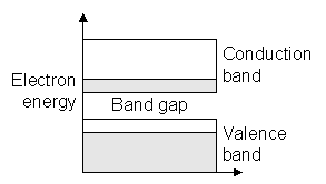
Data Remanence in Semiconductor Devices Peter Gutmann IBM T.J.Watson Research Center pgut001@cs.auckland.ac.nz Abstract A paper published in 1996 examined the problems involved in truly deleting data from magnetic storage media and also made a mention of the fact that similar problems affect data held in semiconductor memory. This work extends the brief coverage of this area given in the earlier paper by providing the technical background information necessary to understand remanence issues in semiconductor devices. Data remanence problems affect not only obvious areas such as RAM and non-volatile memory cells but can also occur in other areas of the device through hot-carrier effects (which change the characteristics of the semiconductors in the device), electromigration (which physically alter the device itself), and various other effects which are examined alongside the more obvious memory-cell remanence problems. The paper concludes with some design and device usage guidelines which can be useful in reducing remanence effects. 1. Introduction to Semiconductor PhysicsElectrons surrounding an atomic nucleus have certain well-defined energy levels. When numbers of atoms are grouped together, the energy levels fall into certain fixed bands made up of the discrete energy levels of individual electrons. Between the bands are empty band gaps in which no electrons are to be found. A band which is completely empty or full of electrons cannot conduct (for an electron to move it must move to a higher discrete energy state, but in a completely full band this can’t happen so a completely full band can conduct just as little as a completely empty one). An electron which is partaking in conduction is said to be in the conduction band, which lies immediately above the valence band. At very low temperatures, the valence band for a semiconductor is full and the conduction band is empty, so that the semiconductor behaves like an insulator. As energy is applied, electrons move across the band gap from the valence band into the conduction band, leaving behind a hole which behaves like a positive charge carrier equal in magnitude to that of the electron as shown in Figure 1. Both the conduction and valence bands can conduct (via electrons or holes), producing a bipolar (two-carrier) conductor. In insulators the band gap is large enough that no promotion of electrons can occur. Conversely, conductors have conduction and valence bands which touch or even overlap.
Figure 1: Electron behaviour in semiconductors In order to make use of a semiconductor, we need to be able to produce material which carries current either through electrons or through holes, but not both. This is done by introducing impurities (usually called dopants) into the semiconductor lattice. For example adding boron (with three valence electrons) to silicon (with four valence electrons) leaves a deficiency of one electron per added boron atom, which is the same as one hole per boron atom. Conversely, adding phosphorus (with five valence electrons) leaves a surplus of one electron. Material doped to conduct mostly by holes is referred to as p-type; material doped to conduct mostly by electrons is called n-type.
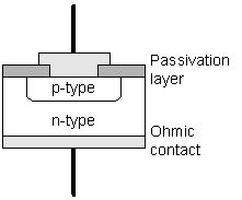
Figure 2: P-N junction diode The makeup of a simple semiconductor device, the P-N junction diode, is illustrated in Figure 2. This consists of an n-type substrate with a p-type layer implanted into it. Protecting the surface is a thermally-grown oxide layer which serves to passivate and protect the silicon (this passivation layer is sometimes referred to as a tamperproof coating in smart card vendor literature). The p-type layer is formed by diffusing a dopant into the substrate at high temperatures through a hole etched into the passivation layer, or through ion-implantation. When such a device is forward biased (a positive voltage applied to the p-type layer and a negative voltage applied to the n-type layer), current flows through the device. When the device is reverse-biased, very little current flows (at least until the device breakdown voltage is reached). The exact mechanism involved is fairly complex, further details are available from any standard reference on the topic [[1]].
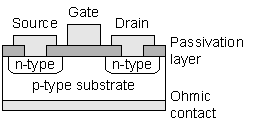
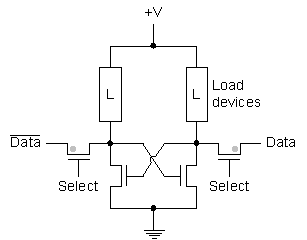
Figure 3: n-channel MOSFET The semiconductor device used in almost all memories and in the majority of VLSI devices is the field-effect transistor (FET), specifically the metal oxide semiconductor FET (MOSFET). The structure of an n-channel MOSFET, a standard building block of semiconductor memories, is shown in Figure 3. When a voltage is applied to the gate, a conducting electron inversion layer is formed underneath it, giving this particular device the name of n-channel MOSFET. The n-type regions at the source and drain serve to supply electrons to the inversion layer during its formation, and the inversion layer, once formed, serves to connect the source and drain. Increasing the gate voltage increases the charge on the inversion layer and therefore the source-drain current. Enhancement-mode devices work in this manner, depletion-mode devices conduct with no gate voltage applied and require an applied voltage to turn them off. Current flow in MOSFETs is dominated by electron/hole drift, and since electrons are more mobile than holes the fastest devices can be obtained by using n-channel devices which move electrons around. Because there are certain circuit advantages to be gained from combining n- and p-channel variants, many circuits use both in the form of complementary MOS (CMOS). Again, more details can be found in any standard reference [[2]]. 2. Semiconductor MemoriesHaving covered the basic building blocks used to create memories, we can now go into the makeup of the memory devices themselves. In practice we distinguish between two main memory types, static RAM (SRAM) in which information is stored by setting the state of a bistable flip-flop which remains in this state as long as power is applied and no new data are written, and dynamic RAM (DRAM) in which information is stored by charging a capacitor which must be refreshed periodically as the charge bleeds away (a later section will cover EEPROM-based non-volatile memories). Because of their more complex circuitry, SRAMs typically only allow 25% of the density of DRAMs, but are sometimes preferred for their faster access times and low-power operation [[3]]. 2.1. SRAMSRAM cells are typically made up of cross-coupled inverters using the structure shown in Figure 4. The load devices can be polysilicon load resistors in older R-load cells, enhancement or depletion mode MOSFETs in an NMOS cell, or PMOS MOSFETs in a CMOS cell (providing an example of the previously mentioned combination of n-and p-channel MOSFET parts in a circuit). The purpose of the load devices is to offset the charge leakage at the drains of the data storage and cell selection MOSFETs. When the load is implemented with PMOS MOSFETs, the resulting CMOS cell has virtually no current flowing through it except during switching, leading to a very low power consumption.
Figure 4: SRAM memory cell Operation of the cell is very simple:
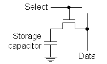
When the cell is selected, the value written via Data/ 2.2. DRAMDRAM cells are made up of some device performing the function of a capacitor and transistors which are used to read/write/refresh the charge in the capacitors. Early designs used three-transistor (3T) cells, newer ones use a one-transistor (1T) cell as shown in Figure 5. Data is stored in the cell by setting the data line to a high or low voltage level when the select line is activated. Compare the simplicity of this circuit to the six-transistor SRAM cell!
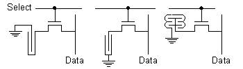
Figure 5: DRAM memory cell The tricky parts of a DRAM cell lie in the design of the circuitry to read out the stored value and the design of the capacitor to maximise the stored charge/minimise the storage capacitor size. Stored values in DRAM cells are read out using sense amplifiers, which are extremely sensitive comparators which compare the value stored in the DRAM cell with that of a reference cell. The reference cell used is a dummy cell which stores a voltage halfway between the two voltage levels used in the memory cell (experimental multilevel cells use slightly different technology which won’t be considered here). Later improvements in sense amplifiers reduced sensitivity to noise and compensated for differences in threshold voltages among devices. 3. DRAM Cell StructureAs has already been mentioned, the second tricky part of DRAM cell design is the design of the cell’s storage capacitor. This typically consists of the underlying semiconductor serving as one plate, separated from the other polysilicon plate by a thin oxide film. This fairly straightforward two-dimensional cell capacitor was used in planar DRAM cells covering the range from 16 kb to 1 Mb cells, and placed the capacitor next to the transistor, occupying about a third of the total cell area. Although some gains in capacitance (leading to a shrinking of cell area) could be made by thinning the oxide thickness separating the capacitor plates, for newer cells it was necessary to move from the 2D plate capacitor structure to 3D structures such as trench and stacked capacitors. The conventional storage time (meaning the time during which the cell contents can be recovered without access to specialised equipment, typically 2-4 seconds [[4]]) for the memory cell is based on storage capacity and therefore the physical dimensions of the capacitor [[5]], so that DRAM designers have used various ingenious tricks to keep the capacitor storage constant while continuously shrinking cell dimensions. Most of the earlier 4 Mb cells used trench capacitors, which had the advantage that capacitance could be increased by deepening the trench, which didn’t use up any extra surface area. Newer generations of trench capacitor cells (sometimes called inverted trench cells) placed the storage electrode inside the trench, which reduced various problems encountered with the earlier cells which had the storage electrode in the substrate. There are a large number of variations possible with this cell, all of them based around the best way to implement the trench capacitor, with some relevant examples shown in Figure 6. The final evolution of the trench cell stacked the transistor above the capacitor, reducing the total area still further at the cost of increasing the number of steps required in the manufacturing process.
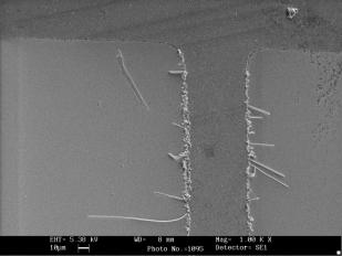
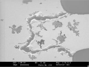
Figure 6: DRAM cells: Trench (left), inverted trench (middle), stacked (right) Newer DRAM cells of 16 Mb and higher capacity moved from a menagerie of trench capacitor types to stacked capacitor cells (STCs), which stack the storage capacitor above the transistor rather than burying it in the silicon underneath. STCs used varying types of horizontal or vertical fins to further increase the surface area, and thus the capacitance. The cell at the right of Figure 6 employs a double-stacked STC. Another alternative to fins is spread-stacking, in which capacitors for different cells are layered over one another. As with trench capacitors, many further capacitor design variants exist [[6]][[7]]. 4. Factors Influencing RAM Cell and General Device OperationNow that we’ve covered the makeup of the various memory cell types, we can look at what makes it possible to analyse and recover data from these cells and from semiconductor devices in general long after it should (in theory) have vanished. To see how this is possible, we need to go back to the level of semiconductor device physics. Recall the discussion of (theoretical) electron/hole flow, in which electrons or holes move freely through a semiconductor lattice. In practice it isn’t nearly this simple, since the lattice will contain impurities, atoms missing from the lattice (vacancies), and extra atoms in the lattice (interstitials). In addition, the atoms in the lattice will be vibrating slightly, producing phonons which work like electrons but carry momentum and can affect electrons if they collide with them. If perchance these various impediments to free hole/electron movement don’t take effect, or because of other factors such as high temperatures or voltages, electrons can build up quite a bit of momentum, which can be transferred to atoms in the lattice during collisions. In some cases this is enough to physically move the atom to new locations, a process known as electromigration. 4.1. ElectromigrationElectromigration involves the relocation of metal atoms due to high current densities, a phenomenon in which atoms are carried along by an “electron wind” in the opposite direction to the conventional current flow, producing voids at the negative electrode and hillocks and whiskers at the positive electrode (if there’s a passivation layer present the excess matter extrudes out to form a whisker, if not it distributes itself to minimise total surface area and forms a hillock). Void formation leads to a local increase in current density and Joule heating (the interaction of electrons and metal ions to produce thermal energy), producing further electromigration effects. When the external stress is removed, the disturbed system tends to relax back to its original equilibrium state, resulting in a backflow which heals some of the electromigration damage. In the long term though this can cause device failure (the excavated voids lead to open circuits, the grown whiskers to short circuits), but in less extreme cases simply serves to alter a device’s operating characteristics in noticeable ways. For example the excavations of voids leads to increased wiring resistance, and the growth of whiskers leads to contact formation and current leakage. An example of a conductor which exhibits whisker growth due to electromigration is shown in Figure 7, and one which exhibits void formation (in this case severe enough to have lead to complete failure) is shown in Figure 8. Electromigration is a complex topic, an excellent introduction to the subject is contained in the survey paper by Lloyd [[8]].
Figure 7: Whisker growth on a conductor due to electromigration In order to reduce electromigration effects which occur in pure metals, interconnects are typically alloys (a few percent copper in aluminium interconnects, a few percent tin in copper interconnects) which have electromigration characteristics of their own in that the Cu or Sn solute atoms are displaced by the electron wind until the source region becomes depleted and behaves like the original pure metal. This initial level of electromigration effect, which doesn’t affect circuit operation and isn’t directly visible, can be detected using electron microprobe techniques which measure the distribution of the Cu or Sn along the base metal line [[9]].
Figure 8: Void formation in a conductor due to electromigration Although recent trends in clock speeds and device feature size reduction are resulting in devices with characteristics such as thin, sub-1.0μm lines, short sub-50-100μm line lengths, and utilisation of high frequencies which have traditionally been regarded as electromigration-resistant [[10]][[11]], they merely provide an ameliorative effect which is balanced by other (in some cases yet-to-be-understood) electromigration phenomena which occur as device dimensions shrink. Even the move to copper interconnects is no panacea, since although the actual copper electromigration mechanisms differ somewhat from those in aluminium, the problem still occurs [9][[12]][[13]]. 4.2. Hot CarriersHigh-energy electrons can cause other problems as well. A very obvious one is that the device heats up during operation because of collisions with the atoms in the lattice, at least one effect of the heating being the generation of further high-speed electrons. A problem which is particularly acute in MOSFETs with very small device dimensions is that of hot carriers which are accelerated to a high energy due to the large electric fields which occur as device dimensions are reduced (hot-carrier effects in newer high-density DRAMs have become so problematic that the devices contain internal voltage converters to reduce the external 3.3 or 5V supply by one or two volts to help combat this problem, and the most recent ones use a supply voltage of 2.5V for similar reasons). In extreme cases these hot electrons can overcome the Si-SiO2 potential barrier and be accelerated into the gate oxide and stay there as excess charge [[14]]. The detrapping time for the resulting trapped charge can range from nanoseconds to days [[15]], although if the charge makes it into the silicon nitride passivation layer it’s effectively there permanently (one study estimated a lifetime in excess of 30 years at 150°C) [[16]]. This excess charge changes the characteristics of the device over time, reducing the on-state current in n-MOSFETs and increasing the off-state current in p-MOSFETs [[17]][[18]][[19]]. The change in characteristics produces a variety of measurable effects, for example one study found a change of several hundred millivolts in memory cell signal voltage over a period of a few minutes [[20]]. This effect is most marked when a 1 bit is written after a 0 bit has been repeatedly read or written from the cell, leading to a drop in the cell threshold voltage. Writing a 0 over a 1 leads to an increase in the cell voltage. One way to detect these voltage shifts is to adjust the settings of the reference cell in the sense amplifier so that instead of being set to a median value appropriate for determining whether a stored value represents a 0 or a 1, it can be used to obtain a precise measurement of the actual voltage from the cell. Hot-carrier stressing of cells can also affect other cell parameters such as the cell’s access and refresh times. For example the precharge time (the time in which it takes to set the DRAM data lines to their preset values before an access) is increased by hot-carrier degradation, although the specific case of precharge time change affects only older NMOS cells and not newer CMOS ones. In addition hot carriers can produce visible or near-infrared photon emission in saturated FETs [[21]][[22]], but use of this phenomenon would require that an attacker be physically present while the device is being operated. Hot carrier effects occur in logic circuits in general and not just in RAM cells. When MOS transistors are employed in digital logic, the logic steady states are regions of low stress because there is either a high field near the drain but the gate is low and the channel is off, or the electric field near the drain is low, in both cases leading to no generation of hot carriers. Hot carriers are generated almost exclusively during switching transitions [[23]][[24]]. The effects of the hot-carrier stressing can be determined by measuring a variety of device parameters, including assorted currents, voltages, and capacitances for the device [[25]]. 4.3. Ionic ContaminationThe most common ionic contamination present in semiconductors arises from the sodium (and to a lesser extent potassium) ions present in materials used during the semiconductor manufacturing and packaging process, a typical ion count being 1010/cm2. This contamination was originally thought to arise from sodium diffusion from the furnace tube [[26]] but with current manufacturing processes comes about because of impurities in the metallisation layers contaminating the silicon beneath. The problem is generally addressed through the standard application of passivation layers to protect the silicon [[27]]. Sodium ions have a fairly high mobility in silicon dioxide, and in the presence of an electric field or elevated temperatures will migrate towards the silicon/silicon dioxide interface in the device, reducing the threshold voltage of n-channel devices and increasing it for p-channel devices [[28]], again producing results which are detectable using the techniques described for hot-carrier effect detection. There has been almost no work done in this area, probably because it isn’t a significant enough problem to affect normal device operation, although one of the few works in this area indicate that it would take many minutes to hours of stress at standard operating temperatures (50-100°C) to produce any noticeable effect [26]. In addition it’s unlikely that the effects of sodium contamination in current devices will be useful in recovering data from them, since reliability studies of devices indicate that contamination occurs only in randomly-distributed locations where impurities have penetrated the passivation layer through microfractures or pinholes [[29]]. Finally, the combination of improved manufacturing and passivation processes and shrinking device dimensions (which reduce the effects of mobile ions on the device) render this an area which is unlikely to bear much fruit. Halide ions are another type of contaminant which may be introduced during the manufacturing process (in some cases deliberately as a semiconductor dopant), however these only lead to general corrosion of the device rather than producing any effects useful for recovering data from it (yet another reason why passivation layers are used is to provide some level of protection against this type of contamination and its attendant side-effects). 4.4. Other EffectsThe storage capacitor in a DRAM cell typically needs to store 250-300 fC of charge. As has already been mentioned, earlier planar cells were scaled down by reducing the oxide thickness in the planar capacitor, while newer cells have gone to 3D structures such as trench and stacked capacitors. Trench capacitors typically used silicon dioxide (often referred to as ONO) insulators, while STCs have gone to using silicon nitride films which have a higher dielectric constant and allow thinner films to be used (as usual, a variety of other exotic technologies are also in use). In both cases parameters such as leakage current and time-dependant dielectric breakdown (TDDB) are relatively static and can’t be used for stored data recovery purposes. Radiation can also affect the operation of a RAM cell, for example radiation-induced charging of a MOSFET’s gate oxide can alter the turn-on voltage of the device, with the oxide-trapped charge shifting the required turn-on voltage at the gate downwards for an n-channel MOSFET, effectively making it easier to turn on. p-channel MOSFETs, because of their slightly different mode of operation, are more resistant to radiation, but when affected become more difficult to turn off. Radiation can therefore alter memory cell parameters such as voltage level thresholds, timings, and power supply and leakage currents. As with DRAM capacitor effects this provides little practical help with stored data recovery, although it can be used to modify the operation of circuits for active attacks — as the radiation level increases it leads to losses in switching speed, a so-called “logic failure” in which a change in logic state becomes impossible. One way to utilise this in an attack would be to irradiate a cell until any erase-on-tamper functionality is rendered unusable, which is why high-end tamper-responsive crypto devices include sensors to detect the presence of ionising radiation [[30]]. A final problem area which is familiar to anyone who has examined the problems of erasing data stored on magnetic media is the fact that some of the more sophisticated memory designs include facilities to map out failing or failed cells in the same way that hard drives will map out bad sectors. This is performed using spare row/column line substitution (SLS), which substitutes problem cells with spare, redundant ones [[31]]. This technology is fairly rare and is usually applied only to correct initial hard failures so it isn’t really a major concern, however it does become a problem in EEPROM/flash storage which is examined in Section 6. 4.5. Methods for Determining Changes in Device OperationThe techniques covered in the literature for determining changes in device operation are many and varied, which is both a blessing because there are so many to choose from and a curse because no two authors can agree on which criteria to use to determine a change in a device’s operation, although there is general agreement that a device’s characteristics have been altered once it has experienced a 100 mV shift in the device threshold voltage or a 10% change in transconductance, voltage, or current (depending on the author’s preferences). Similarly, published results on phenomena such as hot-carrier effects are often obtained with specially-constructed test structures (ring oscillators are popular) which may not apply to other circuits such as memory cells. Because of the wide variation in experimental methods and sources reported in the literature and the equally large variety of devices in use it’s not possible to provide definitive information on how the data recovery process might proceed, this section will attempt to cover some of the more common methods used for determining changes in device operation but is by no means exhaustive. In the most extreme cases it may be possible to recover data directly from the device without resorting to any special techniques. “Burn-in” of data which had been stored in SRAM over long periods of time was common in 1980’s devices, in one reported case DES master keys stored in a hardware security module used for PIN-processing were recovered almost intact on power-up, with recoverability of the remaining bits being aided by the presence of the DES key parity bits [[32]]. More recent SRAM devices are less likely to exhibit this problem to such a degree, requiring the use of more sophisticated readout methods. One widely-used technique from the field of device testing involves examining the amount of power supply current being supplied to the device, known as IDDQ testing. The testing methodology involves executing a set of test vectors until a given location is reached (know as a parametric measurement stopping place or PM stop), at which point the device is halted and the current measured. In the quiescent state, n- and p-channel MOSFETS are either on or off, so there should be no current flowing, and PM stops are selected to coincide with this. Devices which aren’t functioning normally will exhibit abnormal IDDQ characteristics which can be measured once the PM stop is reached. By varying parameters such as the applied voltage and operating temperature, it’s possible to identify devices which have been subject to effects such as hot-carrier stressing which have altered their operational parameters. Floating-gate designs may also have time-dependant IDDQ characteristics in which the floating gate causes both n- and p-channel MOSFETS to be partially on and therefore conducting, a current flow which slowly ceases as the floating gate charges to a logic state and the current subsides. Again, the initial charge (or lack thereof) on the gate and the change in charge can be observed by observing the IDDQ [[33]][[34]]. Many alternative techniques, arising from the field of semiconductor reliability analysis, also exist [[35]]. For example measuring the substrate current, the gate current, and the current in the gated drain-substrate diode of a MOSFET can all be used to determine the amount of stressing which has taken place [[36]][[37]]. These measurements can be used to determine the level and duration of stress applied [[38]]. Access to internal portions of a device can be obtained in many ways [[39]]. Most current ICs employ design for test (DFT) methodologies which break the device up into more manageable blocks of circuitry and provide test access to each block. Other techniques such as bond pad probing can also be used to obtain access to portions of a device. When it becomes necessary to go beyond the access points provided by the manufacturer, things get a bit more tricky. Traditionally, access to internal portions of IC circuitry has been performed with mechanical probing techniques using tungsten wire etched down to a tip radius of 0.1–0.2 μm. These probes provide gigahertz bandwidths with an effective loading capacitance as low as 100 fF and a load resistance of 1 MΩ or more. The recent use of deep submicron designs has complicated mechanical probing, since the optical diffraction limit and small depth of focus of the optical microscopes used to position the probes has made it difficult to see and probe the deep submicron lines. In addition standard mechanical probing isn’t able to access buried lines in devices with multiple metallisation layers. Both of these limits can be overcome through the use of focused ion beam (FIB) workstations, which can be used both to expose buried conductors and to deposit new, easily-accessible probe points on an existing device [[40]] (this technique was used by the Canadian reverse-engineering lab Chipworks to rebuild an ATMEL EEPROM from a crashed aircraft in order to recover data from it [[41]]). The top metal layers are typically broad power buses, so no serious harm is caused by FIB milling of small holes to access lower-layer conductors. The only potential problem is that the FIB process can cause local charging of the device surface, which is usually avoided by grounding all pins in the device and shielding surrounding areas with conducting tape, however the FIB-induced charging can still affect floating gates so it’s a good idea to avoid performing FIB surgery in their general vicinity [[42]]. In addition some technologies such as trench and STC DRAM cells are naturally resistant to being accessed in this manner, although it’s still possible to get to transistors indirectly connected with the cell, for example the ones in the sense amplifiers. 5. Minimising RAM Data RecoverabilityThe previous sections have shown a variety of ways in which stored data can leave traces of its existence behind. These include the effects of electrical stress on ionic contaminants and hot-carrier effects (which can be used to recover overwritten data or data from memory to which power has been removed), and electromigration effects (which can be used to determine, after indefinite time periods, which type of signal was most commonly carried by a particular part of a circuit). The latter would prove useful in recovering information such as the bit patterns of keys stored in special-purpose cryptographic devices — since the physical device is modified the bits can be recovered an arbitrary amount of time later even if the memory cells they were stored in have been successfully erased and trapped charges have bled away. The solution to the first problem is to ensure that sensitive data is stored for as short a time as possible; the solution to the second problem is more difficult but in general involves ensuring that a multitude of signals are sent through circuits without any one signal predominating. These approaches are explained in more detail in the following two sections. 5.1. Avoiding Short-term Retention EffectsThe best way to avoid short-term retention effects is to ensure that no memory cell holds a data value for more than a certain amount of time. Based on the figures given earlier, a few minutes of storage of a given value should be treated as an upper bound; storage for any larger amount of time will cause detectable effects in the memory cell, although it may take quite a while longer before these effects really become a problem. In a series of tests carried out on a sample of SRAM devices, changes in device threshold voltage, transconductance, and drain-source current were observed after 100–500 seconds of stress, leading to a corresponding change in SRAM access time and operating voltage [[43]]. As the SRAM cell in Figure 4 indicates, reads and writes of 0 and 1 bits stress different access transistors in the cell so that it’s possible to determine whether a 0 or 1 was stored there by determining which transistor was stressed the most (the grey dots in the figure indicate the main stress locations). The change in cell behaviour can be determined by recording the cell access time, through voltage microprobing of the cell’s transistors, or using some of the other techniques mentioned earlier. Similar tests have been performed on DRAMs, although in this case the emphasis was on stress effects on shared circuitry such as address buffers and sense amplifiers. While there were quite noticeable effects in all of these areas the study didn’t examine the effect on individual storage cells [[44]]. If nothing is done, the device will eventually recover by itself, although this can take quite some time at normal room temperatures. One way to accelerate the recovery process is to expose the device to elevated temperatures, the read access times for the SRAM devices mentioned previously were found to recover after around 1 ˝ hours at 75°C, 3 days at 50°C, nearly two months at 20°C, and approximately 3 years at 0°C. No recovery was observed for write access times, but given that determining this would involve writing to the cells of interest it’s unlikely that this presents much of a threat. The best practical way to avoid long-term storage effects is to periodically flip the stored bits as suggested in the 1996 paper [[45]] so that each cell never holds a value long enough for it to be “remembered”. Although impractical for large amounts of data, this may be feasible for small amounts of sensitive data such as cryptovariables. For example consider an encryption key whose bits are flipped once a minute. The key flip state is held in keyState, initially set to 0, and access is protected though a mutex keyMutex. The code to flip and use the bits is shown in Figure 9.
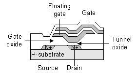
Figure 9: Flipping (left) and using (right) in-memory cryptovariables This can be implemented as a simple wrapper around an existing encryption function, and ensures that the same key bits are never stored in a RAM cell for more than a certain amount of time, in this case one minute. A rather simpler solution which doesn’t require complex bit-flipping and tracking of cryptovariable state information involves moving the data around in memory occasionally and overwriting the original storage locations, again ensuring that data is never stored in a RAM cell for too long. If the luxury of custom circuitry is available (for example in a specialised crypto processor or module), it may be possible to integrate this bit-flipping into the memory circuitry. At each DRAM refresh cycle, the complement of the read value is written. When data is read from the cell, it is XORed with the keyState variable which tracks the state of the data currently stored in the cells (for older 3T cells in which the output data were inverted compared to the input data, it would have been possible to achieve this bit-flipping effect automatically by omitting the data inversion which is normally required during a refresh cycle). Since SRAMs don’t have a DRAM-style refresh cycle, this type of circuit modification isn’t really possible for them, so that performing bit-flipping in an SRAM would require the addition of DRAM-style refresh circuitry, negating most of the advantages of SRAM. Mention should also be made of hybrid memory types which combine DRAM with a small amount of SRAM (usually acting as some form of cache or I/O buffer) to improve the average access speed of the DRAM. A common example of this is extended data out (EDO) DRAM, which places a D-type latch on the data line so that the next access cycle can be started as soon as the data has entered the latches. Since these latches are shared across the entire DRAM, there is little chance of any piece of data except the last one read before a long break in accesses to the DRAM remaining in them for more than an instant, and if this is really a concern they can be flushed with a read to an innocuous memory location. Synchronous DRAMs (SDRAMs), which parallel load a quantity of data into a shift register and then shift it out one bit at a time, have similar properties. 5.2. Avoiding Long-term Retention EffectsLong-term retention effects are most likely to occur when the same data is repeatedly fed through a circuit, an example being the repeated use of a private key in a crypto accelerator for large-integer maths. This is a phenomenon which only occurs in specialised hardware, since general-purpose processors are fed such a variety of data that none of it has much effect on the circuitry. In contrast a private key stored in tamper-resistant hardware and fed repeatedly through a crypto processor will lead to some circuits always carrying the same signals, leading to long-term hot-carrier degradation and electromigration effects. The most common solution to this problem (and that of device protection in general), embedding the crypto device in a tamper-resistant or tamper-sensing package which zeroises the cryptovariables when tampering is detected, is of little help since it’s currently not possible to quickly zeroise electromigration effects, at least not without resorting to chemical zeroisation means. One way of undoing the effects of electromigration (apart from hoping that the system will eventually relax back to its ground state) is to apply a reverse current which reverses the electromigration stress, effectively undoing the electromigration damage [[46]][[47]]. This technique is already used in some EEPROM/flash devices to reduce erase stress by applying a reverse-polarity pulse after an erase pulse [[48]]. A somewhat more complex and difficult-to-implement approach is to have the crypto processor process dummy data when it isn’t working with real data and keys. A downside of this is that it requires that a crypto operation be interruptible once started (it’s no good having to wait for a dummy RSA decrypt to complete each time you want to decrypt data), and leads to increased power consumption and decreased device lifetime. In addition, it assumes that the device isn’t occupied at all times with handling real data, leaving no chance to process any dummy data. Unfortunately alternating dummy and real data is complicated by the design of typical crypto devices. For example encryption hardware will typically contain multiple key registers from which the currently selected key is expanded into storage reserved for the scheduled key, which is then used to encrypt a block of data. This means that switching keys incurs the overhead of a key schedule (although many devices, particularly DES hardware, will do an on-the-fly key schedule which is effectively free in hardware). In addition, pipelined implementations of block ciphers are generally not interruptible, requiring completion of processing of the current block (and in some cases several more blocks to force the pipeline to be flushed) before a key change can take effect. In order to economise on chip real estate (and therefore on device cost), virtually all real-world/non-research DES hardware implementations iterate a single round 16 times, with on-the-fly key scheduling. Non-DES iterated algorithms (as well as non-crypto algorithms such as MD5 and SHA-1) are also implemented by iterating one round rather than by unrolling the operation. These can (with a little redesign) be interrupted at any point in the encryption/decryption cycle and new data can be substituted. In addition the fact that a single round is reused with multiple sets of key bits means that there’s a very mixed set of data patterns in use which minimises the effects of any one pattern. The crypto cores of large-integer maths accelerators (for example RSA accelerators) are less vulnerable to long-term effects since they typically iterate a simple operation such as addition or bit shifting in a loop to achieve multiplication, exponentiation, or whatever else is required. For example a typical RSA accelerator [[49]] might consist of one of more 512- or 1024-bit adders and/or shift registers which are used to perform RSA encryption using a series of squaring and modular multiplication steps, with a 1024-bit multiplication being performed with 1024 additions. Since the operations reuse the basic add/shift circuitry with constantly-changing bit patterns, the problem of data retention in these parts of the circuit are greatly reduced. However, the iterated application of the same keying data exacerbates the retention problem in other parts of the circuit, since a single modular exponentiation can result in key components travelling over the same data paths thousands or even millions of times. The RSA accelerator mentioned above, and others like it, perform a 1 kb modular multiplication with 1k modular additions, and a modular exponentiation with 1k modular multiplications, for a total of 1M applications of the same cryptovariables per RSA operation, and potentially trillions of applications per day of operation in a loaded SSL server. 6. EEPROM Memory CellsFlash memory and EEPROMs are closely related, with flash being simply an extension of EEPROM technology to allow higher densities in exchange for some loss in flexibility. All EEPROM/flash memory cells work in the same general manner and employ as storage element a MOS transistor with a floating gate into which electrons are tunnelled using a process known as Fowler-Nordheim tunnelling, a quantum-mechanical effect in which electrons tunnel through the energy barrier of a very thin dielectric such as silicon dioxide [[50]]. 6.1. FLOTOX CellsA typical older EEPROM technology is Intel’s floating-gate tunnelling oxide (FLOTOX) technology, with a typical transistor structure shown in Figure 10. A cross-section of the device with the corresponding energy-band diagram is shown in Figure 11. To store a charge, the control gate’s voltage is raised with the source and drain grounded, so that electrons tunnel through to the floating gate. To remove the charge, the process is reversed and the electrons tunnel back out. The stored charge changes the threshold of the MOS transistor which comprises the cell, typically by 3–3.5V for a 5V cell [[51]]. The change in the threshold depends on a number of factors including the programming time (the longer the time, the larger the change), temperature (the higher the temperature, the fewer the available hot electrons available to be injected), and the condition of the cell, which is covered in more detail further on.
Figure 10: Typical EEPROM memory cell This example of cell operation is merely representative, the details vary from manufacturer to manufacturer [[52]]. In particular, some issues like dielectric scaling effects and various program and erase mechanisms aren’t fully understood yet, leading to a variety of technologies and continual changes in those technologies. In addition the interpretation of what represents a stored 0 or 1 varies from device to device in that cells can be written into either state, with one state being regarded as “programmed” and the other as “erased”. In some cells the low-stored-charge state is called programmed, in others it’s called erased.
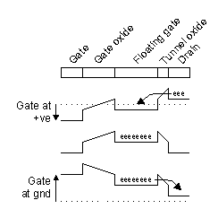
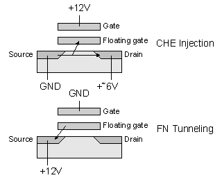
Figure 11: FLOTOX EEPROM program/erase process 6.2. ETOX CellsA somewhat newer technology is represented by Intel’s EPROM tunnel oxide (ETOX) cell [[53]][[54]], which uses channel hot electron (CHE) injection to store a value and Fowler-Nordheim tunnelling to remove it, is illustrated in Figure 12. This technique is widely used in flash memory, although the widely-used NAND flash again uses tunnelling for both programming and erasure (NAND flash cells have a somewhat specialised architecture which allows the use of the more efficient tunnelling for program and erase [[55]]).
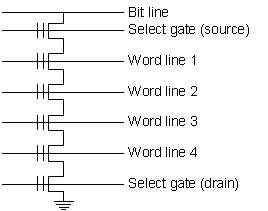
Figure 12: ETOX EEPROM program/erase process The basic EEPROM cell consists of the storage transistor described above and a second transistor to select or deselect the cell (some technologies employ additional error detection and correction circuitry). In an attempt to increase storage density, manufacturers have moved towards using the select transistors to handle multiple storage cells. When the cells are organised in this manner only the programming step can be done in a bit-by-bit basis, the erase operation works by erasing all cells in a block and programming the new data bits as required (or rewriting the old data in sections where no change is to occur). Because programming is possible on a bit by bit basis, it’s usual to only program cells which are currently in the erased state to avoid overprogramming already-programmed cells and (in the case of flash memory) to avoid having to erase an entire sector just to change one or two bytes. The details of the erase operation again vary somewhat across different manufacturers, and unlike programming the erase operation functions on a block of cells at a time. Since the cells aren’t all uniform, a cell array may contain fast-erasing bits as well as typical-erase bits, so that a single erase pulse may not erase all the cells. Because of this it’s necessary to verify the erase and reapply the erase pulse to catch the remaining cells. This operation is repeated until all cells have been reduced to less than the cell erase verify level. In practice the erasure process is a speculative one, with the initial pulse being far shorter than the typical erase time, followed by longer and longer pulses as required. The reason for using this erase process is that we want to avoid further affecting already-erased cells, once a cell is erased by a pulse any subsequent pulses don’t significantly change its threshold voltage. The programming process is usually performed using a similar type of algorithm, with the main difference being that programming is possible on a bit-by-bit basis so that cells which are already at the required level aren’t programmed further [[56]][[57]]. 6.3. Flash Memory TechnologyThe simplest flash technology, employing a NOR structure, allows access to individual cells but requires a dual-voltage supply and has a rather low block density. More common is a NAND structure in which multiple transistors in series are controlled by a single select transistor as shown in Figure 13. NAND EEPROM/flash moves data to and from storage in large blocks, typically 64–256 bytes at a time, and has cells which are typically one-quarter the size of equivalent conventional EEPROM cells. Other size optimisations include tricks such as stacking the select transistor atop the storage transistor and similar methods for merging the function of the two transistors into a single, smaller unit, for example including the select gate as a second gate in the cell, the sidewall select-gate or SISOS cell [[58]]. Another way to improve density is to use multilevel storage, which distinguishes between multiple charge levels in a cell instead of just the basic programmed and erased states [[59]][[60]].
Figure 13: NAND flash memory structure 6.4. Data Remanence in EEPROM/Flash MemoryThe number of write cycles possible with EEPROM technology is limited because the floating gate slowly accumulates electrons, causing a gradual increase in the storage transistor’s threshold voltage which manifests (in its most observable form) as increased programming time and, eventually, an inability to erase the cell. Although EEPROM/flash cells can typically endure 1M or more write/erase cycles, the presence of slight defects in the tunnelling oxide (leading to leakage and eventual breakdown during the tunnelling process) reduces the effective life of the entire collection of cells to 10–100k write/erase cycles. This problem is significantly reduced in flash memory cells, where the main failure mode appears to be negative charge trapping (that is, the trapping of holes in the gate oxide) which inhibits further CHE injection and tunnelling, changing the write and erase times of the cell and shifting its threshold voltage [[61]][[62]]. The amount of trapped charge can be determined by measuring the gate-induced drain leakage (GIDL) current of the cell [[63]], or its effects can be observed more indirectly by measuring the threshold voltage of the cell. In older devices which tied the reference voltage used to read the cell to the device supply voltage it was often possible to do this (and perform other interesting tricks such as making a programmed cell appear erased and vice versa) by varying the device supply voltage, but with newer devices it’s necessary to change the parameters of the reference cells used in the read process, either by re-wiring portions of the cell circuitry or by using undocumented test modes built into the device by manufacturers. A less common failure mode which occurs with the very thin tunnel oxides used in flash memory is one where unselected erased cells adjacent to selected cells gain charge when the selected cell is written (known as a programming disturb) due to the gate of the unselected transistor being stressed by the voltage applied to the common data line shared with the selected transistor. There are various subfamilies of programming disturbs including bitline (also called drain-) and word line (also called gate-) disturbs, in which bias on the common bit or word line causes charge to be injected from the substrate into the floating gate of an unselected cell [[64]][[65]]. This isn’t enough to change the cell threshold sufficiently to upset a normal read operation, but should be detectable using the specialised techniques described above. There is also a type of disturb which can occur when extensive read cycles are performed, with this type of disturb holes are generated in the substrate via impact ionisation and injected into the floating gate, causing a loss of charge. This appears to only affect so-called fast-programming cells [[66]] (which erase and program a lot quicker than typical cells) and isn’t useful in determining the cell contents since it requires knowledge of the cell’s pre-stress characteristics to provide a baseline to compare the post-stress performance to. In terms of long-term retention issues, there is a phenomenon called field-assisted electron emission in which electrons in the floating gate migrate to the interface with the underlying oxide and from there tunnel into the substrate, causing a net charge loss. The opposite occurs with erased cells, in which electron injection takes place [[67]]. Finally, just as with DRAM cells, EEPROM/flash cells are also affected by ionic contamination since the negatively-charged floating gate attracts positive ions which induce charge loss, although the effect is generally too miniscule to be measurable. The means of detecting these effects is as for RAM cells and MOSFET devices in general, for example measuring the change in cell threshold, gate voltage, or observing other phenomena which can be used to characterise the cell’s operation. The changes are particularly apparent in virgin and freshly-programmed cells, where the first set of write/erase cycles causes a (comparatively) large shift in the cell thresholds, after which changes are much more gradual [52][65] (as usual, this is device-dependant, for example the high injection MOS or HIMOS cell exhibits somewhat different behaviour than FLOTOX and ETOX cells [[68]]). Because of this it’s possible to differentiate between programmed-and-erased and never-programmed cells, particularly if the cells have only been programmed and erased once, since the virgin cell characteristics will differ from the erased cell characteristics. Another phenomenon which helps with this is overerasing, in which an erase cycle applied to an already-erased cell leaves the floating gate positively charged, thus turning the memory transistor into a depletion-mode transistor. To avoid this problem, some devices first program all cells before erasing them (for example Intel’s original ETOX-based devices did this, programming the cells to 0s before erasing them to 1s [54]), although the problem is more generally solved by redesigning the cell to avoid excessive overerasing, however even with this protection there’s still a noticeable threshold shift when a virgin cell is programmed and erased. EEPROM/flash memory can also have its characteristics altered through hot carriers which are generated by band-to-band tunnelling and accelerated in the MOSFET’s depletion region, resulting in changes in the threshold voltages of erased cells. As with other factors which affect EEPROM/flash cells, the changes are particularly apparent in fresh cells but tend to become less noticeable after around 10 program/erase cycles [61]. Finally, as with SLS features in RAM, EEPROM/flash memory often contains built-in features which allow the recovery of data long after it should have, in theory, been deleted. The mapping out of failing sectors which parallels the sector sparing used in disk drives has already been mentioned, there also exist device-specific peculiarities such as the fact that data can be recovered from the temporary buffers used in the program-without-erase mode employed in some high-density flash memories, allowing recovery of both the new data which was written and the original data in the sector being written to [60]. Working at a slightly higher level than the device itself are various filesystem-level wear-levelling techniques which are used to decrease the number of erase operations which are necessary to update data, and the number of writes to a single segment of flash [[69]]. Flash file systems are generally log-structured file systems which write changed data to a new location in memory and garbage-collect leftover data in the background or as needed, with the exact details being determined by a cleaning policy which determines which memory segments to clean, when to clean them, and where to write changed data [[70]][[71]][[72]]. Because of this type of operation it’s not possible to cycle fresh cells to reduce remanence effects without bypassing the filesystem, in fact the operation of the wear-levelling system acts to create a worst-case situation in which data is always written to fresh cells. Trying to burn in an area of storage by creating a file and overwriting it 10-100 times will result in that many copies of the data being written to different storage locations, followed by the actual data being written to yet another fresh storage location. Even writing enough data to cycle through all storage locations (which may be unnecessarily painful when the goal is to secure a 1 kB data area on a device containing 256 MB of non-critical data) may not be sufficient, since pseudorandom storage location selection techniques can result in some locations being overwritten many times and others being overwritten only a handful of times. There is no general solution to this problem, since the goal of wear-levelling is the exact opposite of the (controlled) wearing which is needed to avoid remanence problems. Some possible application-specific solutions could include using direct access to memory cells if available, or using knowledge of the particular device- or filesystem’s cleaning policy to try and negate it and provide the required controlled wearing. Since this involves bypassing the primary intended function of the filesystem, it’s a somewhat risky and tricky move. 7. ConclusionAlthough the wide variety of devices and technologies in use, and the continuing introduction of new technologies not explicitly addressed in this work, make providing specific guidelines impossible, the following general design rules should help in making it harder to recover data from semiconductor memory and devices: · Don’t store cryptovariables for long time periods in RAM. Move them to new locations from time to time and zeroise the original storage, or flip the bits if that’s feasible. · Cycle EEPROM/flash cells 10-100 times with random data before writing anything sensitive to them to eliminate any noticeable effects arising from the use of fresh cells (but see also the point further down about over-intelligent non-volatile storage systems). · Don’t assume that a key held in RAM in a piece of crypto hardware such as an RSA accelerator, which reuses the same cryptovariable(s) constantly, has been destroyed when the RAM has been cleared. Hot-carrier and electromigration effects in the crypto circuitry could retain an afterimage of the key long after the original has leaked away into the substrate. · As a corollary, try and design devices such as RSA accelerators which will reuse a cryptovariable over and over again in such a way that they avoid repeatedly running the same signals over dedicated data lines. · Remember that some non-volatile memory devices are a little too intelligent, and may leave copies of sensitive data in mapped-out memory blocks after the active copy has been erased. Devices and/or filesystems which implement wear-levelling techniques are also problematic since there’s no way to know where your data is really going unless you can access the device at a very low level. Finally, however, the best defence against data remanence problems in semiconductor memory is, as with the related problem of data stored on magnetic media, the fact that ever-shrinking device dimensions (DRAM density is increasing by 50% per year [[73]]), and the use of novel techniques such as multilevel storage (which is being used in flash memory and may eventually make an appearance in DRAM as well [[74]]) is making it more and more difficult to recover data from devices. As the 1996 paper suggested for magnetic media, the easiest way to make the task of recovering data difficult is to use the newest, highest-density (and by extension most exotic) storage devices available. Acknowledgements The author would like to thank Steve Weingart and the referees for their feedback and comments on this paper and Dr.Veng-cheong Lo for permission to reproduce the electromigration images. References [[2]] “Fundamentals of Modern VLSI Devices”, Yuan Taur and Tak Ning, Cambridge University Press, 1998. [[3]] “Semiconductor Memories: Technology, Testing, and Reliability”, Ashok Sharma, IEEE Press, 1997. [[4]] “DRAM Variable Retention Time”, P.Restle, J.Park, and B.Lloyd, International Electron Devices Meeting (IEDM’92) Technical Digest, December 1992, p.807. [[5]] “A Numerical Analysis of the Storage Times of Dynamic Random-Access Memory Cells Incorporating Ultrathin Dielectrics”, Alex Romanenko and W.Milton Gosney, IEEE Transactions on Electron Devices, Vol.45, No.1 (January 1998), p.218. [[6]] “Advanced Cell Structures for Dynamic RAMs”, Nicky Lu, IEEE Circuits and Devices Magazine, Vol.5, No.1 (January 1989), p.27. [[7]] “DRAM Technology Perspective for Gigabit Era”, Kinam Kim, Chang-Gyu Hwang, and Jong Gil Lee, IEEE Transactions on Electron Devices, Vol.45, No.3 (March 1998), p.598. [[8]] “Electromigration for Designers: An Introduction for the Non-Specialist”, J.Lloyd, http://www.simplex.com/udsm/whitepapers/electromigration1/index.html. [[9]] “In situ scanning electron microscope comparison studies on electromigration of Cu and Cu(Sn) alloys for advanced chip interconnects”, K.Lee, C.Hu, and K.Tu, Journal of Applied Physics, Vol.78, No.7 (1 October 1995), p.4428. [[10]] “Electromigration in Metals”, Paul Ho and Thomas Kwok, Reports on Progress in Physics, Vol.52, Part 1 (1989), p.301. [[11]] “Theoretical and Experimental Study of Electromigration”, Jian Zhao, “Electromigration and Electronic Device Degradation”, John Wiley and Sons, 1994, p.167. [[12]] “On the unusual electromigration behaviour of copper interconnects”, E.Glickman and M.Nathan, Journal of Applied Physics, Vol.80, No.7 (1 October 1996), p.3782. [[13]] “Surface Electromigration in Copper Interconnects”, N.McCusker, H.Gamble, and B.Armstrong, Proceedings of the International Reliability Physics Symposium (IRPS 1999), March 1999, p.270. [[14]] “Hot-Carrier Effects in MOS Devices”, Eiji Takeda, Cary Yang, and Akemi Miura-Hamada, Academic Press, November 1995. [[15]] “Dynamic Degradation in MOSFET’s — Part I: The Physical Effects”, Martin Brox and Werner Weber, IEEE Transactions on Electron Devices, Vol.38, No.8 (August 1991), p.1852. [[16]] “Data Storage in NOS: Lifetime and Carrier-to-Noise Measurements”, Bruce Terris and Robert Barrett, IEEE Transactions on Electron Devices, Vol.42, No.5 (May 1995), p.944. [[17]] “How do Hot Carriers Degrade N-Channel MOSFETs?”, Kaizad Mistry and Brian Doyle, IEEE Circuits and Devices, Vol.11, No.1 (January 1995), p.28. [[18]] “Hot-carrier Damage in AC-Stressed Deep Submicrometer CMOS Technologies”, A.Bravaix, D.Doguenheim, N.Revil, and E.Vincent, IEEE Integrated Reliability Workshop (IRW’99) Final Report, October 1999, p.61. [[19]] “Hot-carrier Degradation Evolution in Deep Submicrometer CMOS Technologies”, A.Bravaix, IEEE Integrated Reliability Workshop (IRW’99) Final Report, October 1999, p.174. [[20]] “Reduction of Signal Voltage of DRAM Cell Induced by Discharge of Trapped Charges in Nano-meter Thick Dual Dielectric Film”, J.Kumagai, K.Toita, S.Kaki, and S.Sawada, Proceedings of the International Reliability Physics Symposium (IRPS 1990), April 1990, p.170. [[21]] “Extended (1.1-2.9eV) Hot-Carrier Induced Photon Emission in n-Channel MOSFETs”, M.Lanzoni, E.Sangiorgi, C.Fiegna, and B.Riccň, International Electron Devices Meeting (IEDM’90) Technical Digest, December 1990, p.69. [[22]] “Time-Resolved Optical Characterisation of Electrical Activity in Integrated Circuits”, James Tsang, Jeffrey Kash, and David Vallett, Proceedings of the IEEE, Vol.88, No.9 (September 2000), p.1440. [[23]] “Setting the Trap for Hot Carriers”, Shian Aur, Charvaka Duvvury, and William Hunter, IEEE Circuits and Devices, Vol.11, No.4 (July 1995), p.18. [[24]] “Design Considerations for CMOS Digital Circuits with Improved Hot-Carrier Reliability”, Yusuf Leblebici, IEEE Journal of Solid-state Circuits, Vol.31, No.7 (July 1996), p.1014. [[25]] “Hot-Carrier-Induced Alterations of MOSFET Capacitances: A Quantitative Monitor for Electrical Degradation”, David Esseni, Augusto Pieracci, Manrico Quadrelli, and Bruno Riccň, IEEE Transactions on Electron Devices, Vol.45, No.11 (November 1998), p.2319. [[26]] “Mobile ion effects in low-temperature silicon oxides”, N.Young, A.Gill, and I.Clarence, Journal of Applied Physics, Vol.66, No.1 (1 July 1989), p.187. [[27]] “Built-in Reliability Through Sodium Elimination”, Jeff Chinn, Yueh-Se Ho, and Mike Chang, Proceedings of the International Reliability Physics Symposium (IRPS 1994), April 1994, p.249. [[28]] “Failure Modes and Mechanisms for VLSI ICs — A Review”, Fausto Fantini and Carlo Morandi, IEE Proceedings — Part G: Electronic Circuits and Systems, Vol.132, No.3 (June 1985), p.74. [[29]] “An Accelerated Sodium Resistance Test for IC Passivation Films”, Charlie Hong, Brent Henson, Tony Scelsi, and Robert Hance, Proceedings of the International Reliability Physics Symposium (IRPS 1996), May 1996, p.318. [[30]] “Building a High-Performance, Programmable Secure Coprocessor”, Sean Smith and Steve Weingart, Computer Networks, Vol.31, No.4 (April 1999), p.831. [[31]] “Memory LSI Reliability”, Masao Fukuma, Hiroshi Furuta, and Masahide Takada, Proceedings of the IEEE, Vol.81, No.5 (May 1993), p.768. [[32]] “Low Cost Attacks on Tamper Resistant Devices”, Ross Anderson and Markus Kuhn, Proceedings of the 5th International Workshop on Security Protocols, Springer-Verlag LNCS No.1361, April 1997. [[33]] “IDDQ Testing for High Performance CMOS — The Next Ten Years”, T.Williams, R.Kapur, M.Mercer, R.Dennard, and W.Maly, Proceedings of the European Design and Test Conference (EDTC’96), 1996, p.578. [[34]] “Electrical Characterization”, Steven Frank, Wilson Tan, and John West, in “Failure Analysis of Integrated Circuits: Tools and Techniques”, Kluwer Academic Publishers, 1999, p.13. [[35]] “Semiconductor Material and Device Characterization (2nd Ed)”, Dieter Schroder, John Wiley and Sons, 1998. [[36]] “Characterization of Hot-Electron-Stressed MOSFET’s by Low-Temperature Measurements of the Drain Tunnel Current”, Alexandre, Acovic, Michel Dutoit, and Marc Ilegems, IEEE Transactions on Electron Devices, Vol.37, No.6 (June 1990), p.1467. [[37]] “Monitoring Trapped Charge Generation for Gate Oxide Under Stress”, Yung Hao Lin, Chung Len Lee, and Tan Fu Lei, IEEE Transactions on Electron Devices, Vol.44, No.9 (September 1997), p.1441. [[38]] “Characteristic length and time in electromigration”, Morris Shatzkes and Yusue Huang, Journal of Applied Physics, Vol.74, No.11 (December 1993), p.6609. [[39]] “IC Failure Analysis: Techniques and Tools for Quality and Reliability Improvement”, Jerry Soden and Richard Anderson, Proceedings of the IEEE, Vol.81, No.5 (May 1993), p.703. [[40]] “The role of focused ion beams in physical failure analysis”, G.Matusiewicz, S.Kirch, V.Seeley, and P.Blauner, Proceedings of the International Reliability Physics Symposium (IRPS 1991), April 1991, p.167. [[42]] “Probing Technology for IC Diagnosis”, Christopher Talbot, in “Failure Analysis of Integrated Circuits: Tools and Techniques”, Kluwer Academic Publishers, 1999, p.113. [[43]] “Relation between the hot carrier lifetime of transistors and CMOS SRAM products”, Jacob van der Pol and Jan Koomen, Proceedings of the International Reliability Physics Symposium (IRPS 1990), April 1990, p.178. [[44]] “Hot-carrier-induced Circuit Degradation in Actual DRAM”, Yoonjong Huh, Dooyoung Yang, Hyungsoon Shin, and Yungkwon Sung, Proceedings of the International Reliability Physics Symposium (IRPS 1995), April 1995, p.72. [[45]] “Secure Deletion of Data from Magnetic and Solid-State Memory”, Peter Gutmann, Proceedings of the 6th Usenix Security Symposium, July 1996, p.77. [[46]] “Metal Electromigration Damage Healing Under Bidirectional Current Stress”, Jiang Tao, Nathan Cheung, and Chenming Ho, IEEE Electron Device Letters, Vol.14, No.12 (December 1993), p.554. [[47]] “An Electromigration Failure Model for Interconnects Under Pulsed and Bidirectional Current Stressing”, Jiang Tao, Nathan Cheung, and Chenming Ho, IEEE Transactions on Electron Devices, Vol.41, No.4 (April 1994), p.539. [[48]] “New Write/Erase Operation Technology for Flash EEPROM Cells to Improve the Read Disturb Characteristics”, Tetsuo Endoh, Hirohisa Iizuka, Riichirou Shirota, and Fujio Masuoka, IEICE Transactions on Electron Devices, Vol.E80-C, No.10 (October 1997), p.1317. [[49]] “A High-Speed RSA Encryption LSI with Low Power Dissipation”, A.Satoh, Y.Kobayashi, H.Niijima, N.Ooba, S.Munetoh, and S.Sone, Proceedings of the Information Security Workshop (ISW’97), Springer-Verlag LNCS No.1396, September 1997. [[50]] “Nonvolatile Semiconductor Memory Technology: A Comprehensive Guide to Understanding and Using NVSM Devices”, William Brown and Joe Brewer (eds), IEEE Press, 1998. [[51]] “Hot-electron injection into the oxide in n-channel MOS devices”, Boaz Eitan and Dov Frohman-Bentchkowsky, IEEE Transactions on Electron Devices, Vol.28, No.3 (March 1981), p.328. [[52]] “Analysis and Modeling of Floating-gate EEPROM Cells”, Avinoam Kolodny, Sidney Nieh, and Boaz Eitan, IEEE Transactions on Electron Devices, Vol.33, No.6 (June 1986), p.835 [[53]] “An In-System Reprogrammable 256K CMOS Flash Memory”, Virgil Kynett, Alan Baker, Mickey Fandrich, George Hoekstra, Owen Jungroth, Jerry Kreifels, and Steven Wells, Proceedings of the IEEE International Solid State Circuits Conference, February 1988, p.132. [[54]] “An In-System Reprogrammable 32K×8 CMOS Flash Memory”, Virgil Kynett, Alan Baker, Mick Fandrich, George Hoekstra, Owen Jungroth, Jerry Kreifels, Steven Wells, and Mark Winston, IEEE Journal of Solid-state Circuits, Vol.23, No.5 (October 1988), p.1157. [[55]] “New Ultra High Density EPROM and Flash EPROM Cell with NAND Structure”, Fujio Masuoka, Masaki Momodomi, Yoshihisa Iwata, and Riichirou Shirota, International Electron Devices Meeting (IEDM’87) Technical Digest, 1987, p.552. [[56]] “A 4-Mb NAND EEPROM with Tight Programmed Vt Distribution”, Masaki Momodomi, Tomoharu Tanaka, Yoshihisa Iwata, Yoshiyuki Tanaka, Hideko Oodaira, Yasuo Itoh, Riichirou Shirota, Kazunori Ohuchi, and Fujio Masuoka, IEEE Journal of Solid-state Circuits, Vol.26, No.4 (April 1991), p.492. [[57]] “A Quick Intelligent Page-Programming Architecture and a Shielded Bitline Sensing Method for 3V-Only NAND Flash Memory”, Tomoharu Tanaka, Yoshiyuki Tanaka, Hiroshi Nakamura, Koji Sakui, Hideko Oodaira, Riichirou Shirota, Kazunori Ohuchi, Fujio Masuoka, and Hisashi Hara, IEEE Journal of Solid-state Circuits, Vol.29, No.11 (November 1994), p.1366. [[58]] “Flash Memory Cells — An Overview”, Paolo Pavan, Roberto Bez, Piero Olivo, and Enrico Zanoni, Proceedings of the IEEE, Vol.85, No.8 (August 1997), p.1248. [[59]] “A multilevel-cell 32Mb flash memory”, M.Bauer, R.Alexis, B.Atwood, K.Fazio, K.Frary, M.Hensel, M.Ishac, J.Javanifard, M.Landgraf, D.Leak, K.Loe, D.Mills, P.Ruby, R.Rozman, S.Sweha, K.Talreja, and K.Wojciechowski, Proceedings of the IEEE International Solid State Circuits Conference, February 1995, p.132. [[60]] “A 256-Mb Multilevel Flash Memory with 2-MB/s Program Rate for Mass Storage Applications”, Atsushi Nozoe, Hiroaki Kotani, Tetsuya Tsujikawa, Keiichi Yoshida, Kazunori Furusawa, Masataka Kato, Toshiaki Nishimoto, Hitoshi Kume, Hideaki Kurata, Naoki Miyamoto, Shoji Kubono, Michitaro Kanamitsu, Kenji Koda, Takeshi Nakayama, Yasuhiro Kouro, Akira Hosogane, Natsuo Ajika, and Kiyoteru Kobayashi, IEEE Journal of Solid-state Circuits, Vol.34, No.11 (November 1999), p.1544. [[61]] “Degradations due to Hole Trapping in Flash Memory Cells”, Sameer Haddad, Chi Chang, Balaji Swaminathan, and Jih Lien, IEEE Electron Device Letters, Vol.10, No.3 (March 1989), p.117. [[62]] “Degradation of Tunnel-Oxide Floating-Gate EEPROM Devices and the Correlation with High Field-Current-Induced Degradation of Thin Gate Oxides”, Johan Witters, Guido Groeseneken, and Herman Maes, IEEE Transactions on Electron Devices, Vol.36, No.9 (September 1989), p.1663. [[63]] “Determination of Trapped Oxide Charge in Flash EPROMs and MOSFETs with Thin Oxides”, K.Tamer San and Tso-Ping Ma, IEEE Electron Device Letters, Vol.13, No.8 (August 1992), p.439. [[64]] “Reliability Issues of Flash Memory Cells”, Seiichi Aritome, Riichiro Shirota, Gertjan Hemink, Tetsuo Endoh, and Fujio Masuoka, Proceedings of the IEEE, Vol.81, No.5 (May 1993), p.776. [[65]] “Effects of Erase Source Bias on Flash EPROM Device Reliability”, K.Tamer San, Çetin Kaya, and T.P.Ma, IEEE Transactions on Electron Devices, Vol.42, No.1 (January 1995), p.150. [[66]] “Flash EPROM Disturb Mechanisms”, Clyde Dunn, Çetin Kaya, Terry Lewis, Tim Strauss, John Schreck, Pat Hefly, Matt Middendorf, and Tamer San, Proceedings of the International Reliability Physics Symposium (IRPS 1994), April 1994, p.299. [[67]] “Retention characteristics of single-poly EEPROM cells”, C.Papadas, G.Ghibaudo, G.Pananakakis, C.Riva, P.Ghezzi, C.Gounelle, and P.Mortini, Proceedings of the European Symposium on Reliability of Electron Devices, Failure Physics and Analysis, October 1991, p.517. [[68]] “Write/Erase Degradation in Source Side Injection Flash EEPROMs: Characterization Techniques and Wearout Mechanisms”, Dirk Wellekens, Jan Van Houdt, Lorenzo Faraone, Guido Groeseneken, and Herman Maes, IEEE Transactions on Electron Devices, Vol.42, No.11 (November 1995), p.1992. [[70]] “Non-volatile memory for fast, reliable file systems”, Mary Baker, Satoshi Asami, Etienne Deprit, John Ouseterhout and Margo Seltzer, Proceedings of the Fifth International Conference on Architectural Support for Programming Languages and Operating Systems (ASPLOS-V), October 1992, p.10. [[71]] “A Flash-Memory Based File System”, Atsuo Kawaguchi, Shingo Nishioka, and Hiroshi Motoda, Proceedings of the 1995 Usenix Technical Conference, January 1995. [[72]] “Cleaning policies in mobile computers using flash memory”, M.-L. Chiang and R.-C. Chang, Journal of Systems and Software, Vol.48, No.3 (1 November 1999), p.213. |
|
This paper was originally published in the
Proceedings of the 10th USENIX Security Symposium,
August 13–17, 2001, Washington, D.C., USA
Last changed: 2 Jan. 2002 ml |
|