Nitin Agrawal![]() , Vijayan Prabhakaran, Ted Wobber,
, Vijayan Prabhakaran, Ted Wobber,
John D. Davis, Mark Manasse, Rina Panigrahy
Microsoft Research, Silicon Valley
*University of Wisconsin, Madison
The advent of the NAND-flash based solid-state storage device (SSD) is certain to represent a sea change in the architecture of computer storage subsystems. These devices are capable of producing not only exceptional bandwidth, but also random I/O performance that is orders of magnitude better than that of rotating disks. Moreover, SSDs offer both a significant savings in power budget and an absence of moving parts, improving system reliability.
Although solid-state disks cost significantly more per unit capacity than their rotating counterparts, there are numerous applications where they can be applied to great benefit. For example, in transaction-processing systems, disk capacity is often wasted in order to improve operation throughput. In such configurations, many small (cost inefficient) rotating disks are deployed to increase I/O parallelism. Large SSDs, suitably optimized for random read and write performance, could effectively replace whole farms of slow, rotating disks. At this writing, small SSDs are starting to appear in laptop computers because of their reduced power-profile and reliability in portable environments. As the cost of flash continues to decline, the potential application space for solid-state disks will certainly continue to grow.
Despite the promise that SSDs hold, there is little in the literature about the architectural tradeoffs inherent in their design. Where such knowledge exists, it typically remains the intellectual property of SSD manufacturers. As a consequence, it is difficult to understand the architecture of a given device, and harder still to interpret its performance characteristics.
In this paper, we lay out a range of design tradeoffs that are relevant to NAND-flash solid-state storage. We then analyze several of these tradeoffs using a trace-based disk simulator that we have customized to characterize different SSD organizations. Since we can only speculate about the detailed internals of existing SSDs, we base our simulator on the specified properties of NAND-flash chips. Our analysis is driven by various traces captured from running systems such as a full-scale TPC-C benchmark, an Exchange server workload, and various standard file system benchmarks.
We find that many of the issues that arise in SSD design appear to mimic problems that have previously appeared higher in the storage stack. In solving these hard problems, there is considerable latitude for design choice. We show that the following systems issues are relevant to SSD performance:
As SSDs increase in complexity, existing disk models will become insufficient for predicting performance. In particular, random write performance and disk lifetime will vary significantly due to the locality of disk write operations. We introduce a new model for characterizing this behavior based on cleaning efficiency and suggest a new wear-leveling algorithm for extending SSD lifetime.
The remainder of this paper is organized as follows. In the next section, we provide background on the properties of NAND-flash memory. Section 3 describes the basic functionality that SSD designers must provide and the major challenges in implementing these devices. Section 4 describes our simulation environment and presents an evaluation of the various design choices. Section 5 provides a discussion of SSD wear-leveling and gives preliminary simulator results on this topic. Related work is discussed in Section 6, and Section 7 concludes.
Our discussion of flash memory is based on the latest product specifications for Samsung's K9XXG08UXM series NAND-flash part [29]. Other vendors such as Micron and Hynix offer products with similar features. For the remainder of this paper, we treat the 4GB Samsung part as a canonical exemplar, although the specifics of other vendors' parts will differ in some respects. We present the specifications for single-level cell (SLC) flash. Multi-level cell (MLC) flash is cheaper than SLC, but has inferior performance and lifetime.
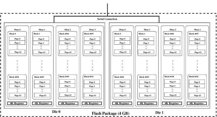
Figure 1 shows a schematic for a flash package. A flash package is composed from one or more dies (also called chips). We describe a 4GB flash-package consisting of two 2GB dies, sharing an 8-bit serial I/O bus and a number of common control signals. The two dies have separate chip enable and ready/busy signals. Thus, one of the dies can accept commands and data while the other is carrying out another operation. The package also supports interleaved operations between the two dies.
Each die within a package contains 8192 blocks, organized among 4 planes of 2048 blocks. The dies can operate independently, each performing operations involving one or two planes. Two-plane commands can be executed on either plane-pairs 0 & 1 or 2 & 3, but not across other combinations. Each block in turn consists of 64 4KB pages. In addition to data, each page includes a 128 byte region to store metadata (identification and error-detection information). Table 1 presents the operational attributes of the Samsung 4GB flash memory.
Writing (or programming) is also done at page granularity by shifting data into the data register (100 μs) and then writing it out to the flash cell (200 μs). Pages must be written out sequentially within a block, from low to high addresses. The part also provides a specialized copy-back program operation from one page to another, improving performance by avoiding the need to transport data through the serial line to an external buffer.
In this paper, we discuss a 2 x 2GB flash package, but extensions to larger dies and/or packages with more dies are straightforward.
The serial interface over which flash packages receive commands and transmit data is a primary bottleneck for SSD performance. The Samsung part takes roughly 100 μs to transfer a 4KB page from the on-chip register to an off-chip controller. This dwarfs the 25 μs required to move data into the register from the NAND cells. When these two operations are taken in series, a flash package can only produce 8000 page reads per second (32 MB/sec). If interleaving is employed within a die, the maximum read bandwidth from a single part improves to 10000 reads per second (40 MB/sec). Writes, on the other hand, require the same 100 μs serial transfer time per page as reads, but 200 μs programming time. Without interleaving, this gives a maximum, single-part write rate of 3330 pages per second (13 MB/sec). Interleaving the serial transfer time and the program operation doubles the overall bandwidth. In theory, because there are two independent dies on the packages we are considering, we can interleave three operations on the two dies put together. This would allow both writes and reads to progress at the speed of the serial interconnect.
Interleaving can provide considerable speedups when the operation latency is greater than the serial access latency. For example, a costly erase command can in some cases proceed in parallel with other commands. As another example, fully interleaved page copying between two packages can proceed at close to 100 μs per page as depicted in Figure 2 in spite of the 200 μs cost of a single write operation. Here, 4 source planes and 4 destination planes copy pages at speed without performing simultaneous operations on the same plane-pair and while optimally making use of the serial bus pins connected to both flash dies. Once the pipe is loaded, a write completes every interval (100 μs).
Even when flash architectures support interleaving, they do so with serious constraints. So, for example, operations on the same flash plane cannot be interleaved. This suggests that same-package interleaving is best employed for a choreographed set of related operations, such as a multi-page read or write as depicted in Figure 2. The Samsung parts we examined support a fast internal copy-back operation that allows data to be copied to another block on-chip without crossing the serial pins. This optimization comes at a cost: the data can only be copied within the same flash plane (of 2048 blocks). Two such copies may themselves be interleaved on different planes, and the result yields similar performance to the fully-interleaved inter-package copying depicted in Figure 2, but without monopolizing the serial pins.
In this section we outline some of the basic issues that arise when constructing a solid-state disk from NAND-flash components. Although we introduce a number of dimensions in which designs can differ, we leave the evaluation of specific choices until Section 4.
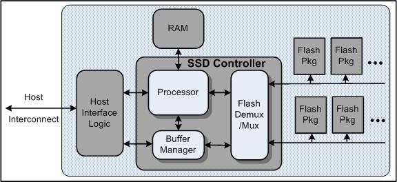
All NAND-based SSDs are constructed from an array of flash packages similar to those described in the previous section. Figure 3 depicts a generalized block diagram for an SSD. Each SSD must contain host interface logic to support some form of physical host interface connection (USB, FiberChannel, PCI Express, SATA) and logical disk emulation, like a flash translation layer mechanism to enable the SSD to mimic a hard disk drive. The bandwidth of the host interconnect is often a critical constraint on the performance of the device as a whole, and it must be matched to the performance available to and from the flash array. An internal buffer manager holds pending and satisfied requests along the primary data path. A multiplexer (Flash Demux/Mux) emits commands and handles transport of data along the serial connections to the flash packages. The multiplexer can include additional logic, for example, to buffer commands and data. A processing engine is also required to manage the request flow and mappings from disk logical block address to physical flash location. The processor, buffer-manager, and multiplexer are typically implemented in a discrete component such as an ASIC or FPGA, and data flow between these logic elements is very fast. The processor, and its associated RAM, may be integrated, as is the case for simple USB flash-stick devices, or standalone as for designs with more substantial processing and memory requirements.
As described in Section 2, flash packages export an 8-bit wide serial data interface with a similar number of control pins. A 32GB SSD with 8 of the Samsung parts would require 136 pins at the flash controller(s) just for the flash components. With such a device, it might be possible to achieve full interconnection between the flash controller(s) and flash packages, but for larger configurations this is not likely to remain feasible. For the moment, we assume full interconnection between data path, control logic, and flash. We return to the issue of interconnect density in Section 3.3.
This paper is primarily concerned with the organization of the flash array and the algorithms needed to manage mappings between logical disk and physical flash addresses. It is beyond the scope of this paper to tackle the many important issues surrounding the design and layout of SSD logic components.
As pointed out by Birrell et al. [2], the nature of NAND flash dictates that writes cannot be performed in place as on a rotating disk. Moreover, to achieve acceptable performance, writes must be performed sequentially whenever possible, as in a log. Since each write of a single logical-disk block address (LBA) corresponds to a write of a different flash page, even the simplest SSD must maintain some form of mapping between logical block address and physical flash location. We assume that the logical block map is held in volatile memory and reconstructed from stable storage at startup time.
We frame the discussion of logical block maps using the abstraction of an allocation pool to think about how an SSD allocates flash blocks to service write requests. When handling a write request, each target logical page (4KB) is allocated from a pre-determined pool of flash memory. The scope of an allocation pool might be as small as a flash plane or as large as multiple flash packages. When considering the properties of allocation pools, the following variables come to mind.
These variables are then bound by three constraints:
The variables that define allocation pools trade off against these constraints. For example, if a large portion of the LBA space is statically mapped, then there is little scope for load-balancing. If a contiguous range of LBAs is mapped to the same physical die, performance for sequential access in large chunks will suffer. With a small logical page size, more work will be required to eliminate valid pages from erasure candidates. If the logical page size (with unit span) is equal to the block size, then erasure is simplified because the write unit and erase unit are the same, however all writes smaller than the logical page size result in a read-modify-write operation involving the portions of the logical page not being modified.
RAID systems [26] often stripe logically contiguous chunks of data (e.g. 64KB or larger) across multiple physical disks. Here, we use striping at fine granularity to distribute logical pages (4K) across multiple flash dies or packages. Doing so serves both to distribute load and to arrange that consecutive pages will be placed on different packages that can be accessed in parallel.
Fleshing out the design sketched by Birrell et al. [2], we use flash blocks as the natural allocation unit within an allocation pool. At any given time, a pool can have one or more active blocks available to hold incoming writes. To support the continued allocation of fresh active blocks, we need a garbage collector to enumerate previously-used blocks that must be erased and recycled. If the logical page granularity is smaller than the flash block size, then flash blocks must be cleaned prior to erasure. Cleaning can be summarized as follows. When a page write is complete, the previously mapped page location is superseded since its contents are now out-of-date. When recycling a candidate block, all non-superseded pages in the candidate must be written elsewhere prior to erasure.
In the worst case, where superseded pages are distributed evenly across all blocks, N-1 cleaning writes must be issued for every new data write (where there are N pages per block). Of course, most workloads produce clusters of write activity, which in turn lead to multiple superseded pages per block when the data is overwritten. We introduce the term cleaning efficiency to quantify the ratio of superseded pages to total pages during block cleaning. Although there are many possible algorithms for choosing candidate blocks for recycling, it is always desirable to optimize cleaning efficiency. It's worth noting that the use of striping to enhance parallel access for sequential addresses works against the clustering of superseded pages.
For each allocation pool we maintain a free block list that we populate with recycled blocks. In this section and the next, we assume a purely greedy approach that calls for choosing blocks to recycle based on potential cleaning efficiency. As described in Section 2, NAND flash sustains only a limited number of erasures per block. Therefore, it is desirable to choose candidates for recycling such that all blocks age evenly. This property is enforced through the process known as wear-leveling. In Section 5, we discuss how the choice of cleaning candidates interacts directly with wear-leveling, and suggest a modified greedy algorithm.
In an SSD that emulates a traditional disk interface, there is no abstraction of a free disk sector. Hence, the SSD is always full with respect to its advertised capacity. In order for cleaning to work, there must be enough spare blocks (not counted in the overall capacity) to allow writes and cleaning to proceed, and to allow for block replacement if a block fails. An SSD can be substantially overprovisioned with such spare capacity in order to reduce the demand for cleaning blocks in foreground. Delayed block cleaning might also produce better clustering of superseded pages in non-random workloads.
In the previous subsection, we stipulated that a given LBA is statically mapped to a specific allocation pool. Cleaning can, however, operate at a finer granularity. One reason for doing so is to exploit low-level efficiency in the flash architecture such as the internal copy-back operation described in Section 2.2, which only applies when pages are moved within the same plane. Since a single flash plane of 2048 blocks represents a very small allocation pool for the purposes of load distribution, we would like to allocate from a larger pool. However, if an active block and cleaning state per plane is maintained, then cleaning operations within the same plane can be arranged with high probability.
It might be tempting to view block cleaning as similar to log-cleaning in a Log-Structured File System [28] and indeed there are similarities. However, apart from the obvious difference that we model a block store as opposed to a file system, a log-structured store that writes and cleans in strict disk-order cannot choose candidate blocks so as to yield higher cleaning efficiency. And, as with LFS-like file systems, it's altogether too easy to combine workloads that would cause all recoverable space to be situated far from the log's cleaning pointer. For example, writing the same sets of blocks over and over would require a full cycle over the disk content in order for the cleaning pointer to reach the free space near the end of the log. And, unlike a log-structured file system, the disk here is always ``full", corresponding to maximal cleaning pressure all the time.
If an SSD is going to achieve bandwidths or I/O rates greater than the single-chip maxima described in Section 2.2, it must be able to handle I/O requests on multiple flash packages in parallel, making use of the additional serial connections to their pins. There are several possible techniques for obtaining such parallelism assuming full connectivity to the flash, some of which we have touched on already.
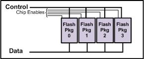
The situation becomes more interesting when full connectivity to the flash packages is not possible. Two choices are readily apparent for organizing a gang of flash packages: 1) the packages are connected to a serial bus where a controller dynamically selects the target of each command; and 2) each package has separate data path to the controller, but the control pins are connected in a single broadcast bus. Configuration (1) is depicted in Figure 4. Data and control lines are shared, and an enable line for each package selects the target for a command. This scheme increases capacity without requiring more pins, but it does not increase bandwidth. Configuration (2) is depicted in Figure 5. Here there is shared set of control pins, but since there are individual data paths to each package, synchronous operations which span multiple packages can proceed in parallel. The enable lines can be removed from the second configuration, but in this case all operations must apply to the entire gang, and no package can lie idle.
Interleaving can play a role within a gang. A long running operation such as block erasure can be performed on one element while reads or writes are proceeding on others (hence the control line need only be held long enough to issue a command). The only constraint is competition for the shared data and command bus. This could become quite important during block recycling since block erasure is an order of magnitude more expensive than other operations.
In another form of parallelism, intra-plane copy-back can be used to implement block cleaning in background. However, cleaning can take place with somewhat lower latency if pages are streamed at maximum speed between two chips. This benefit comes, of course, at the expense of occupying two sets of controller pins for the duration.
It is unlikely that any one choice for exploiting parallelism can be optimal for all workloads, and certainly as SSD capacity scales up, it will be difficult to ensure full connectivity between controllers and flash packages. The best choices will undoubtedly be dictated by workload properties. For example, a highly sequential workload will benefit from ganging, a workload with inherent parallelism will take advantage of a deeply parallel request queuing structure, and a workload with poor cleaning efficiency (e.g. no locality) will rely on a cleaning strategy that is compatible with the foreground load.
Flash memory is by definition persistent storage. However, in order to recover SSD state, it is essential to rebuild the logical block map and all related data structures. This recovery must also reconstruct knowledge of failed blocks so that they are not re-introduced into active use. There are several possible approaches to this problem. Most take advantage of the fact that each flash page contains a dedicated area (128 bytes) of metadata storage that can be used to store the logical block address that maps to a given flash page. In our simulator, we model the technique sketched by Birrell et al. [2]. This technique eliminates the need to visit every page at startup by saving mapping information per block rather than per page. Note that in any such algorithm, pages whose content has been superseded but not yet erased will appear multiple times during recovery. In these cases, the stable storage representation must allow the recovery algorithm to determine the most recent instance of a logical page within an allocation pool.
Flash parts do not, in general, provide error detection and correction. These functions must be provided by application firmware. The page metadata can also hold an error-detection code to determine which pages are valid and which blocks are failure-free, and an error-correction code to recover from the single-bit errors that are expected with NAND flash. Samsung specifies block lifetime assuming the presence of a single-bit ECC [29]. It may be possible to extend block lifetime by using more robust error correction.
The problem of recovering SSD state can be bypassed altogether by holding the logical block map in Phase-Change RAM [14] or Magnetoresistive RAM [9]. These non-volatile memories are writable at byte granularity and don't have the block-erasure constraints of NAND flash. The former is not yet widely available, and the latter can be obtained in small capacities, but at 1000 times the cost of NAND flash. Alternatively, backup power (e.g. big capacitors) might be enough to flush the necessary recovery state to flash on demand.
The market for NAND flash continues to grow both in volume and in breadth as storage capacity increases and cost per unit storage declines. As of late 2007, laptops are available that use an SSD as the primary disk drive. In addition, high-end flash systems have become available for the enterprise marketplace. Most products in the marketplace can be placed into one of three categories.
Consumer portable storage. These are inexpensive units with one or perhaps two flash packages and a simple controller. They commonly appear as USB flash sticks or camera memories, and feature moderate bandwidth for sequential operations, moderate random read performance, and very poor random write performance.
Laptop disk replacements. These disks provide substantial bandwidth to approximate that of the IDE and SATA disks they replace. Random read performance is far superior to that of rotating media. Random write performance is comparable to that of rotating media.
Enterprise/database accelerators. These units promise very fast sequential performance, random read performance superior to that of a high-end RAID array, and very strong random write performance. They have costs to match. However, the specified random-write performance numbers are often a bit mysterious, and sometimes are missing altogether. For example, it is often difficult to tell whether cleaning costs are included.
In Table 2, we provide performance numbers for
sample devices in these categories. The sample devices are the
Lexar JD Firefly 8GB USB flash stick, the MTron MSD-SATA3025
SSD [20], the Zeus![]() SSD [30], and the
FusionIO ioDrive [10]. The MTron device is in the
second category above, while the Zeus and FusionIO devices are
clearly enterprise-class. We are not privy to the internals of
these devices, but we can speculate on how they are organized.
Previous work [2] points out that consumer USB flash
devices almost certainly use a logical page granularity close to
the size of a flash block. Limited random read performance
suggests that only a single I/O request is in flight at a time.
The MTron device gives random read I/O performance better than can
be expected with a single flash request stream, so it almost
certainly employs some sort of parallel request structure.
However, the poor random write I/O performance suggests that a
large logical page size is being used (with substantial
read-modify-write costs). The random write performance of the
Zeus and FusionIO devices suggest a sophisticated block mapping
scheme, and multiple parallel activities are clearly needed to
reach the stated random I/O performance. The Zeus system appears
to lower pressure on its cleaning algorithm by substantial
overprovisioning [7]. The FusionIO system (for
which only a preliminary specification was available in 2007) is
the first to offer a PCI-Express interconnect.
SSD [30], and the
FusionIO ioDrive [10]. The MTron device is in the
second category above, while the Zeus and FusionIO devices are
clearly enterprise-class. We are not privy to the internals of
these devices, but we can speculate on how they are organized.
Previous work [2] points out that consumer USB flash
devices almost certainly use a logical page granularity close to
the size of a flash block. Limited random read performance
suggests that only a single I/O request is in flight at a time.
The MTron device gives random read I/O performance better than can
be expected with a single flash request stream, so it almost
certainly employs some sort of parallel request structure.
However, the poor random write I/O performance suggests that a
large logical page size is being used (with substantial
read-modify-write costs). The random write performance of the
Zeus and FusionIO devices suggest a sophisticated block mapping
scheme, and multiple parallel activities are clearly needed to
reach the stated random I/O performance. The Zeus system appears
to lower pressure on its cleaning algorithm by substantial
overprovisioning [7]. The FusionIO system (for
which only a preliminary specification was available in 2007) is
the first to offer a PCI-Express interconnect.
From our discussion of industry trends, it is clear that current SSDs can get very good performance numbers from ideal workloads. For example, under sequential workloads these devices verge on saturating any interconnect, RAID controller [24], or host peripheral chipset [1]. However, it's unclear whether this is true of a single sequential stream, or multiple streams. And if multiple, how many streams are optimal? Does the stated write performance account for cleaning overhead? What is the random write performance and what are the assumptions about distribution of superseded pages during cleaning?
This section introduces a trace-driven simulation environment that allows us to gain insight into SSD behavior under various workloads.
Our simulation environment is a modified version of the DiskSim simulator [4] from the CMU Parallel Data Lab. DiskSim does not specifically support simulation of solid-state disks, but its infrastructure for processing trace logs and its extensibility made it a good vehicle for customization.
DiskSim emulates a hierarchy of storage components such as buses and controllers (e.g. RAID arrays) as well as disks. We implemented an SSD module derived from the generic rotating disk module. Since this module did not originally support multiple request queues, we added an auxiliary level of parallel elements, each with a closed queue, to represent flash elements or gangs. We also added logic to serialize request completions from these parallel elements. For each element, we maintain data structures to represent SSD logical block maps, cleaning state, and wear-leveling state. As each request is processed, sufficient delay is introduced to simulate real-time delay according to the specifications in Table 1. If cleaning and recycling is called for by the simulator state, additional delay is introduced to account for it, and the state is updated accordingly. We added configuration parameters to enable such features as background cleaning, gang-size, gang organization (e.g. switched or shared-control), interleaving, and overprovisioning.
Verifying our simulation requires detailed experiments to determine the caching and flash-management algorithms used by actual SSD hardware. We intend to do this as future work.
We present results for a collection of workload traces which we name as follows for the purpose of exposition: TPC-C, Exchange, IOzone, and Postmark.
We first examine a synthetic workload generated by DiskSim. We present this workload to characterize baseline behavior for sequential and random access request streams. IOzone [15] and Postmark [16] are standard file system benchmarks run on a workstation class PC with a 750 GB SATA disk. These benchmarks require relatively little capacity, and can be simulated on a single SSD. Despite the fact that we do not simulate on-disk caching, in the above traces, the disk cache was enabled, producing unnaturally low request inter-arrival times for writes.
TPC-C is an instance of the well-established database benchmark [31]. Our trace is a 30-minute trace of a large-scale TPC-C configuration, running 16,000 warehouses. The traced system comprised 14 RAID (HP MSA1500 Fibre-Channel) controllers each supporting 28 high-speed 36 GB disks. We target one of the controllers serving non-log data tables: a mixed read/write workload with about twice as many reads as writes. (The 13 non-log controllers have similar workloads.) Although each controller manages over a terabyte of storage, the benchmark uses only about 160GB per controller. The large number of disks are needed to obtain disk arms that can handle requests in parallel. All requests in this workload are for multiples of 8KB blocks. Alignment is important, since misaligned requests to flash add a page access to every read or write. Several of the logical volumes in our configuration were misaligned, yielding traces in which LBA mod 8 = 7 for all LBA. We corrected for this by post-processing the roughly 6.8M events in this trace.
The Exchange workload is taken from a server running Microsoft Exchange. This is a specialized database workload with about a 3:2 read-to-write ratio. The traced server had 6 non-log RAID controllers of a terabyte each (14 disks). We extracted a 15 minute trace of roughly 65000 events from one of these controllers, involving requests over 250GB of disk capacity.
We first present results from a simple workload synthesized by the DiskSim workload-generator. Then, we vary different configuration parameters and study their impact on SSD performance under the macro benchmarks.
Our baseline configuration is an SSD with 32GB of flash: 8 fully connected flash packages. In this configuration, allocation pools are the size of a flash package, the logical page and stripe size is 4KB, and cleaning requires data transfer across the flash package serial interface. Because we model only a small SSD, the larger workloads require that we simulate a RAID controller as well. We assume that each SSD is overprovisioned by 15%, which means that the disk capacity available to the host is around 27 GB. We invoke cleaning when less than 5% free blocks remain. The TPC-C workload requires 6 attached SSDs in this configuration, and the Exchange workload requires 10.
Microbenchmarks. We ran a set of 6 synthetic microbenchmarks
involving 4 KB I/O operations and report the access latency and
respective I/O rates in Table 3. In a
fully-connected SSD, sequential and random I/Os have equivalent
latencies. Note that this latency includes the time to transfer
both the page data and the 128-byte page metadata. When cleaning
is enabled, the latencies for write operations reflect the
additional overhead. Notice that sequential writes result in
better cleaning efficiency, and therefore less cleaning
overhead.
Page Size, Striping, and Interleaving. Choice of logical
page size has a substantial impact on overall performance. As
discussed in Section 3.1, every write
that is smaller than the logical page size requires a
read-modify-write operation.
When run with a full-block page size (256KB) at
unit depth (e.g., the entire logical page on the same die),
TPC-C produces an average I/O latency of over 20 ms, more than
two orders of magnitude greater than what can be expected with a
4KB page size. Our eight package configuration with a 256KB
page size can (barely) keep up
with the average trace rate of 300 IOPS per SSD, but only due to the
inherent parallelism available in the SSD. We do much better
with a smaller page size. The average latency for TPC-C is
200 μs with a page size of 4KB, although the workload
does not have enough events to test the 40,000 IOPS that this
implies.
As described in Section 2.2, I/O performance can
be improved by interleaving multiple requests within a single
flash package or die. Our simulator accounts for interleaving
by noticing when two requests are queued on a flash package that
can proceed concurrently according to the hardware constraints.
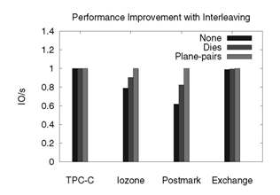
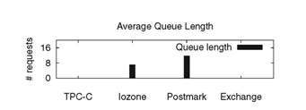
Figure 6(a) presents I/O
rates normalized with respect to our baseline configuration and
shows how various types of
interleaving improves the performance of our baseline
configuration. While IOzone and Postmark show an increase in
throughput, TPC-C and Exchange do not benefit from
interleaving. As shown in Figure 6(b),
the average number of queued requests (per flash package, as measured by DiskSim) is
very close to zero for these two workloads. With no
queuing, interleaving will not occur. IOzone and Postmark have
a significant sequential I/O component. When a large sequential
request is dispatched to multiple packages due to stripe boundaries,
queuing occurs and interleaving becomes beneficial. One might think that TPC-C would
benefit from striping its 8KB requests at 8KB increments thereby
allowing every request to interleave at the package or die
level. However, splitting up each request into parallel 4KB
requests is in this case superior.
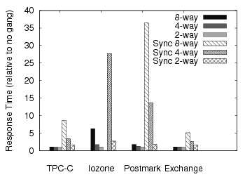
Gang Performance. As suggested in
Section 3.3, ganging flash components offers
the possibility of scaling capacity without linearly scaling pin
density and firmware logic complexity. We proposed two types of
ganging: shared-bus and shared-control.
Table 4 shows the average latency of Exchange
I/O requests (variable size) under 8-wide (32KB) and 16-wide
(64KB) shared-bus gangs. As it happens, this workload requires
only about 900 IOPS, so the 16-gang is fast enough even though
the ganged components have to be accessed serially. There is no
obvious load-balancing problem when simple page-level striping
is used, even though one would expect such problems to be
exacerbated by ganging.
A shared-control gang can be organized in two ways. First, although
the flash packages are ganged, separate allocation and cleaning
decisions can be made on each package, enabling one to perform
opportunistic parallel operations, e.g., when two reads are presented
on different gang members at the same time, they can be performed
concurrently. We refer to this as asynchronous-shared-control
ganging. Second, all packages in a gang can be managed in synchrony
by utilizing a logical page depth equal to that of gang size, e.g.,
a 8-wide gang would have a page size of 32KB, and we call this
design synchronous-shared-control ganging. We use intra-plane
copy-back to implement read-modify-write for writes of less than a page
in synchronous ganging.
Figure 7 presents normalized response time (with respect to the base line configuration) from various synchronous and asynchronous shared-control gang sizes. Since the logical page size of a synchronous gang is bigger than the corresponding asynchronous gang, it limits the number of simultaneous operations that can be performed in a gang unit, and hence synchronous ganging uniformly underperforms when compared to asynchronous ganging. The synchronous 8-way gang could not support the IOzone workload in simulated real-time and hence its result is absent in the Figure 7.
Copy-back vs. Inter-plane Transfer. Cleaning a block
involves moving any valid pages to another block. If the source
and destination blocks are within a plane, pages can be moved
using the copy-back feature without having to transfer them
across the serial pins. Otherwise, pages can be moved between
planes through the serial pins.
Table 5 presents the average number of blocks cleaned per flash package,
the average time to
clean a block, and the average cleaning efficiency. Using the copy-back feature, TPC-C shows a
40% improvement in cleaning cost per block. In spite of the large number blocks being cleaned,
IOzone and Postmark do not show any benefit from copy-back.
These benchmarks produce perfect cleaning efficiency; they move no pages during
cleaning.
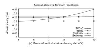
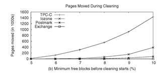
Cleaning Thresholds. An SSD needs a minimum number of free blocks to operate
correctly; for example, free blocks are required to perform data
transfer during cleaning or to sustain sudden bursts of write
requests. Increasing this minimum-block threshold triggers
cleaning earlier and therefore increases observed overhead.
Figure 8(a) shows the variation in access
latency as we increase the free blocks threshold. While the
access latencies increase in TPC-C with the threshold, other
workloads show little difference. This difference in the access
latencies among different workloads is explained by
Figure 8(b), which plots the number
of pages moved during cleaning against the free blocks
threshold. Figures 8(a) and
8(b) show that increasing the
minimum free blocks threshold may affect the overall performance
of the SSD depending upon the pages moved under the
workload.
In the discussion below, we propose a cleaning and wear-leveling algorithm applicable to NAND-flash SSDs. We assume that an SSD implements a block-oriented disk interface which provides no a priori knowledge of optimal data placement or likely longevity.
Efficient cleaning, while it may reduce overall wear, does not translate to even wear. The drawback of choosing a greedy approach (maximal cleaning efficiency) is that the same blocks may get used over and over again and a large collection of blocks with relatively cold content may remain unused. For example, if 50% of the blocks contain cold data that is never superseded, and the rest contains hot data that is modified frequently, then the block to be erased will always be taken from the hot blocks. This will lead to a situation where the life of the hot blocks will be consumed while that of the cold blocks will be unutilized, wasting half the total life of the device.
Our objective is to design a block management algorithm so as to delay the expiry time of any single block; that is, we wish to avoid the situation where one or a few blocks have finished their life when most blocks have much life left. This goal implies that we must ensure that the remaining lifetime across all blocks is equal within an acceptable variance. To this end, we propose tracking the average lifetime remaining over all blocks. The remaining lifetime of any block should be within ageVariance (say 20%) of the average remaining lifetime.
This desired policy can be achieved by running the greedy strategy as long as it picks a page whose remaining lifetime is above the threshold. To do this, we must maintain some notion of block erase count in persistent storage (for example in the metadata portion of the first page). What then should we do for worn out blocks that drop below the threshold? A simple approach is to only allow recycling when a candidate's remaining lifetime exceeds the threshold. Doing this could exclude large numbers of blocks from consideration which in turn would cause the remaining blocks to be recycled more frequently and with poorer cleaning efficiency. For example if 25% of the blocks have cold data and the remaining 75% have hot data accessed uniformly then after a certain number of writes, the latter will get worn out and become ineligible for erasure. Subsequently, recycling will be concentrated on the 25% of the blocks containing cold data. So these blocks will be reused 4 times faster and yield commensurately fewer pages per erasure. Hence, we need to avoid making a large number of blocks ineligible for recycling over an extended period of time.
Instead of freezing the recycling of worn out blocks, we can rate-limit their usage. Randomization can be used here to evenly spread out the effect of a rate-limit on the worn out blocks. We use an approach similar to Random Early Discard [8] in which the probability of recycling drops linearly from 1 to 0 as a block's remaining lifetime drops from say 80% to 0% of the average.
Another way to slow down the usage of worn out blocks is to migrate cold data into old blocks. When data is migrated, cleaning is performed as usual, but then rather than attaching the recycled block to the allocation pool queue, instead data from a cold block is used to fill it. The cold block is then recycled and added to the free queue. This action can be triggered, for example, if the remaining lifetime in a block drops below retirementAge (say 85% of the average remaining lifetime). retirementAge should be less than ageVariance of average remaining lifetime so that cold data can be migrated into a worn out block before rate-limiting kicks in.
One method to identify cold data is to look for blocks that have exceeded specified parameters for remaining lifetime and time since last erasure. This approximation can be made more accurate by keeping track of when a block was last written in its metadata. In this case, it is important that temperature metadata travel with the content as it is moved to a new physical block. When a block is migrated, the migration should not affect its temperature metric. However, the process of cleaning can group pages of different temperatures in the same block, in this case, the resultant block temperature needs to reflect that of the aggregate.
So in summary, we propose running the greedy strategy (e.g., the most superseded pages) for picking the next block to be recycled, as modified below.
We ran IOzone (due to its high cleaning rate) to study the wear-leveling algorithm described above. We reduced the lifetime of a flash block from 100K to 50 cycles for our experiment so that the ageVariance (set to 20%) and retirementAge (set to 85%) thresholds become relevant. Tables 7 and 8 present the results for 3 different techniques: the greedy algorithm, greedy with rate-limited cleaning of worn-out blocks, and greedy with rate-limiting and cold data migration. Although the average block lifetime is similar across the techniques, invoking migration gives a much smaller standard deviation of remaining block lifetimes at the end of the run. Moreover, with migration, there were no block expiries (e.g., blocks over the erasure limit). Since the simple greedy technique does not perform any rate-limiting, fewer blocks reach expiry when rate-limiting is used than without it. Table 8 presents the distribution of flash-block lifetimes around the mean. One can observe that cold data migration offers better clustering around the mean than the other options.
A system that implements a traditional disk-block interface incurs unnecessary overhead by managing disk blocks that are free from the point of view of the file system. Under a random workload, a disk that is half full will have twice the cleaning efficiency of a full disk (and all disks are full except those that are overprovisioned). Previous work on Semantically-Smart Disk Systems [21] has shown the benefits of greater file-system information being available at the disk level. Although SSDs that implement a pure disk interface provide advantages from a perspective of compatibility, it is worth considering whether the SSD API might support the abstraction of an unused block. With such a modification, SSD performance would vary with the percentage of free space rather than always suffering maximal cleaning load and wear.
Cleaning load can be reduced if an SSD has knowledge of content volatility. For example, certain file types such as audio and video files are not often modified. If available at the disk block level, this information would provide a better predictive metric than the history-based approximations above. More importantly, if cold data can be identified a priori, then there is a better chance of establishing locality for warm data, localization of warm data will lead to better cleaning efficiency.
We discuss related work in designing solid-state storage devices, file systems for improving performance, and work on algorithms and data structures for such devices.
Previous work on solid-state storage design has focused on resource-constrained environments such as embedded systems or sensor networks (e.g., Capsule [19], MicroHash [34]). This body of work has largely dealt with small flash devices (up to a few hundred MB), with low-power, shock resistance and size being primary considerations. The MicroHash index [34] attempts to support temporal queries on data stored locally on a flash chip in the presence of a low energy budget. Nath and Kansal propose FlashDB [23], a hybrid B+-tree index design. The key idea is to have different update strategies depending on the frequency of reads and writes: in-place updates for pages that are frequently read or infrequently written, and logging for those that are frequently written.
While the work in embedded and sensor environments has given useful insights into the workings and constraints of solid-state devices, our work systematically explores design issues in high-performance storage systems. In these environments, operation throughput is often the most important metric of interest.
Hybrid disks are another area of research [3] and commercial interest. These devices place a small amount of flash memory alongside a much larger traditional disk to improve performance. Flash is not the final persistent store, but rather a write-cache to improve latency. The non-volatile cache on hybrid disks can be controlled through specific ATA commands [25].
File systems have also used non-volatile memory to log data or requests. WAFL [13] is one such file system that uses non-volatile RAM (NVRAM) to keep a log of NFS requests it has processed since the last consistency point. After an unclean shutdown, WAFL replays any requests in the log to prevent them from being lost.
The hybrid disk and NVRAM approaches use flash as an add-on storage for rotating disks. In our designs, solid-state devices serve as a replacement for rotating disks, providing a better rate of operation throughput.
Kim and Ahn [17] propose a cache-management strategy that improves random-write performance for SSDs operating with a block-sized logical page. They attempt to flush write-cache pages that occupy the same block at the same time, thereby reducing read-modify-write overhead. This works well if the workload does not overwhelm the cache or require immediate write persistence. Moreover, write-caching that handles bursty or repetitive writes is complementary to our approach.
File systems specific to flash devices have also been proposed. Most of these designs are based on Log-structured File Systems [28], as a way to compensate for the write latency associated with erasures. JFFS, and its successor JFFS2 [27], are journaling file systems for flash. The JFFS file systems are not memory-efficient for storing volatile data structures, and require a full scan to reconstruct these data structures from persistent storage upon a crash. JFFS2 performs wear-leveling, in a somewhat ad-hoc fashion, with the cleaner selecting a block with valid data at every 100th cleaning, and one with most invalid data at other times.
YAFFS [18] is flash file system for use in embedded devices. It treats handling of wear-leveling akin to handling bad blocks, which appear as the device gets used. Other examples of embedded micro-controller file systems include the Transactional Flash File System [11] and the Efficient Log Structured Flash File System [6]. The former was designed for more expensive, byte addressable NOR flash memory, which has considerably fewer constraints than NAND flash. The latter was designed for sensor nodes using NAND flash. It supports simple garbage collection and provides an optional best effort crash recovery mechanism.
It is useful to compare our approach with improvements higher up in the storage stack, such as the specialized file systems for flash devices. Enhancements at the flash controller will obviate the need to invest significant effort in re-writing a custom flash file system. It will also alleviate the overhead of transitioning from rotating disks to flash-based storage by exporting a ``flash-disk" that performs well even with existing file systems.
Much prior work has been done on proposing and evaluating algorithms and data structures specially suited for operation in flash devices. A recent survey [12] discusses much of this work in greater detail.
Wear-leveling is an important constraint of flash devices and several proposals have been made to perform it efficiently, increasing the usable life time of the device. Wu and Zwaenepoel [33] use a relative wear-count of blocks for wear-leveling. Similar to our approach, data is swapped when the block chosen for cleaning exceeds a wear-count. Wells [32] proposed a reclamation policy based on weighted combination of efficiency and wear-leveling, while the work by Chiang and Chang [5] uses the likelihood of a block being used soon, which is equivalent to the logical hotness or coldness of data within the block chosen for cleaning.
Recent work by Myers [22] looks at ways to exploit the inherent parallelism offered by the flash chip. He fragments a block and stores it on multiple physical pages on different chips, under the hypotheses that a dynamic striping or replication strategy based on workload will outperform a static one. His work focuses on applicability of flash for database workloads and concludes that widespread adoption is not yet possible. In contrast, our design and analysis shows that while there are several tradeoffs, SSDs are a viable and possibly an attractive option for transactional workloads such as TPC-C.
As we have shown, there are numerous design tradeoffs for SSDs that impact performance. There is also significant interplay between both the hardware and software components and the workload. Our work provides insight into how all of these components must cooperate in order to produce an SSD design that meets the performance goals of the targeted workload. From the hardware standpoint, the SSD interface (SATA, IDE, PCI-Express) and package organization dictate theoretical maximum I/O performance. On the software side, the properties of the allocation pool, load balancing, data placement, and block management (wear-leveling and cleaning) combined with workload characteristics determine overall SSD performance. Moreover, we have demonstrated that all designs can benefit from plane interleaving and some degree of overprovisioning, and we have proposed a wear-leveling algorithm and shown its efficacy in at least one scenario.
We have demonstrated a simulation-based technique for modeling SSD performance driven by traces extracted from real hardware. In some cases, the traced systems require storage components that would be much too expensive for most organizations to provide for the purposes of experimentation. Our simulation framework has proved both resilient and flexible, and we expect to continue to add to the set of behaviors that we can model. Shared-control ganging and refined wear-leveling data are particular topics of interest.
There is no fixed rule that NAND flash be integrated into computer systems as disk storage. However, the block-access nature of NAND suggests that a block-oriented interface will often be appropriate. Although outside of the scope of this work, we suspect that our simulation techniques will be applicable to NAND-flash block-storage independent of architecture because the same issues (e.g. cleaning, wear-leveling) will still arise.
Flash-based storage is certain to play an important role in future storage architectures. One corollary of our simulation results is that the storage systems necessary to support a substantial TPC-C workload, which in the past have involved many hundreds of spindles, might well be replaced in future by small numbers of SSD-like devices. Our work represents a step towards understanding and optimizing the performance of such systems.
We are grateful to the DiskSim team for making their simulator available, and to Dushyanth Narayanan for porting it to Windows. Andrew Birrell, Chuck Thacker, and James Hamilton participated in many fruitful discussions during the course of this work. Bruce Worthington and Swaroop Kavalanekar gathered our TPC-C and Exchange traces. And finally, we would like to honor the memory of Dr. Jim Gray, who inspired this work.
This document was generated using the LaTeX2HTML translator Version 2002-2-1 (1.71)
Copyright © 1993, 1994, 1995, 1996,
Nikos Drakos,
Computer Based Learning Unit, University of Leeds.
Copyright © 1997, 1998, 1999,
Ross Moore,
Mathematics Department, Macquarie University, Sydney.
The command line arguments were:
latex2html -split 0 -show_section_numbers -local_icons -no_navigation main.tex
The translation was initiated by Vijayan Prabhakaran on 2008-04-25